LG Optimus 2X & NVIDIA Tegra 2 Review: The First Dual-Core Smartphone
by Brian Klug & Anand Lal Shimpi on February 7, 2011 3:53 AM EST- Posted in
- Smartphones
- Tegra 2
- LG
- Optimus 2X
- Mobile
- NVIDIA
The GeForce ULV
Complementing the three major CPU architectures in the mobile applications processor market for 2011 there are three major GPUs you’ll see crop up in devices this year: Imagination Technologies’ PowerVR SGX Series5 and Series5XT, Qualcomm’s Adreno 205/220 and NVIDIA’s GeForce ULV. There are other players but these three are the ones that will show up in the most exciting devices this year.
ImgTec licenses its GPUs for use in a number of SoCs. Apple’s A4, TI’s OMAP 3 and 4 and Samsung’s Hummingbird all use ImgTec GPUs. The currently used high end from ImgTec is the PowerVR SGX 540, which features four unified shader pipelines capable of handling both pixel and vertex shader operations. The PowerVR SGX 543 is widely expected to be used in Apple’s 5th generation SoC.
The PowerVR SGX as well as Qualcomm’s Adreno GPUs both implement tile based deferred rendering architectures. In the early days of the PC GPU race deferred renderers were quite competitive. As geometry complexity in games increased, ATI and NVIDIA’s immediate mode rendering + hidden surface removal proved to be the better option. Given the lack of serious 3D gaming, much less geometry heavy titles on smartphones today the tile based approach makes a lot of sense. Tile based renderers conserve both power and memory bandwidth, two things that are in very short supply on smartphones. Remember from our CPU discussions that in many cases only a single 32-bit LPDDR2 memory channel has to feed two CPU cores as well as the GPU. By comparison, even PCs from 10 years ago had a 64-bit memory bus just for the CPU and a 128-bit memory bus for the GPU.
NVIDIA believes that the future of GPUs on smartphones is no different than the future of PC GPUs: immediate mode renderers. As a result, the GeForce ULV GPU in NVIDIA’s Tegra 2 looks very similar to a desktop GPU—just a lot smaller, and a lot lower power. It’s also worth pointing out that until we get PC-like content on smartphones, NVIDIA’s approach to ultra mobile GPU architectures may not always make the most sense for power efficiency.
(Note that some of what follows below is borrowed from our earlier coverage of NVIDIA's Tegra 2):
At a high level NVIDIA is calling the GeForce ULV an 8-core GPU, however its not a unified shader GPU. Each core is an ALU but half of them are used for vertex shaders and the other half are for pixel shaders. You can expect the GeForce ULV line to take a similar evolutionary path to desktop GeForce in the future (meaning it’ll eventually be a unified shader architecture).
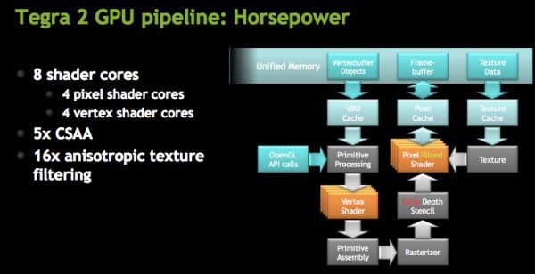
The four vertex shader cores/ALUs can do a total of 4 MADDs per clock, the same is true for the four pixel shader ALUs (4 MADDs per clock).
The GeForce ULV in NVIDIA’s Tegra 2 runs at a minimum of 100MHz but it can scale up to 400MHz depending on the SoC version:
| NVIDIA Tegra 2 | ||||||
| SoC | Part Number | CPU Clock | GPU Clock | Availability | ||
| NVIDIA Tegra 2 | T20 | 1GHz | 333MHz | Now | ||
| NVIDIA Tegra 2 | AP20H | 1GHz | 300MHz | Now | ||
| NVIDIA Tegra 2 3D | T25 | 1.2GHz | 400MHz | Q2 2011 | ||
| NVIDIA Tegra 2 3D | AP25 | 1.2GHz | 400MHz | Q2 2011 | ||
The AP20H runs at up to 300MHz, while the tablet version runs at a faster 333MHz.
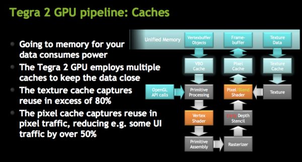
Architecturally, the GeForce ULV borrows several technologies that only recently debuted on desktop GPUs. GeForce ULV has a pixel cache, a feature that wasn’t introduced in GeForce on the desktop until Fermi. This is purely an efficiency play as saving any trips to main memory reduces power consumption considerably (firing up external interfaces always burns watts quicker than having data on die).
NVIDIA also moved the register files closer to the math units, again in the pursuit of low power consumption. GeForce ULV is also extremely clock gated although it’s not something we’re able to quantify.
NVIDIA did reduce the number of pipeline stages compared to its desktop GPUs by a factor of 2.5 to keep power consumption down.
The GeForce ULV supports Early Z culling, a feature first introduced on the desktop with G80. While G80 could throw away around 64 pixels per clock, early Z on GeForce ULV can throw away 4 pixels per clock. While early Z isn’t the equivalent of a tile based renderer, it can close the efficiency gap between immediate mode renderers and TBRs.
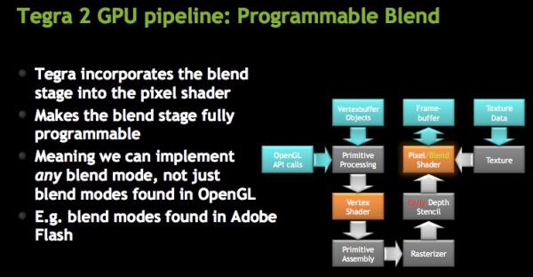
The ROPs are integrated into the pixel shader, making what NVIDIA calls a programmable blend unit. GeForce ULV uses the same ALUs for ROPs as it does for pixel shaders. This hardware reuse saves die size although it adds control complexity to the design. The hardware can perform one texture fetch and one ROP operation per clock.
While GeForce ULV supports texture compression, it doesn’t support frame buffer compression.
Both AA and AF are supported by GeForce ULV. NVIDIA supports 5X coverage sample AA (same CSAA as we have on the desktop) and up to 16X anisotropic filtering.
The performance comparison is far more difficult to quantify in the ultra mobile space than among desktop GPUs. There are some very good 3D games out for Android and iOS, unfortunately none of them have built in benchmarks. There are even those that would make for good performance tests however OEM agreements and politics prevent them from being used as such. At the other end of the spectrum we have a lot of absolutely horrible 3D benchmarks, or games with benchmarks that aren’t representative of current or future game performance. In between the two extremes we have some benchmark suites (e.g. GLBenchmark) that aren’t representative of current or future GPU performance, but they also aren’t completely useless. Unfortunately today we’ll have to rely on a mixture of all of these to paint a picture of how NVIDIA’s GeForce ULV stacks up to the competition.
Just as is the case in the PC GPU space, game and driver optimizations play as large of a role in performance as the GPU architecture itself. NVIDIA believes that its experience with game developers will ultimately give it the edge in the performance race. It’s far too early to tell as most of NVIDIA’s partners aren’t even playing in the smartphone space yet. However if PC and console titles make their way to smartphones, NVIDIA’s experience and developer relationships may prove to be a tremendous ally.


75 Comments
View All Comments
Exophase - Monday, February 7, 2011 - link
Thanks Anand.I'm surprised to hear that shot was from IMG, given that it was an IMG employee who made the comment originally about Tegra's 16-bit banding being evident on it, from the screenshot. Whoops. I do wonder what could be causing this, then.
Nonetheless, while that definitely makes my 16bit color claim invalid the depth buffer one should still hold. We might need to wait and see how much of a difference this actually makes, or rather how effective nVidia's 16-bit depth space is.
I'm glad to hear that you're as concerned about benchmarks on Android as I am. It's especially frustrating when I see people using them to try to indicate Atom being substantially better clock for clock than Cortex-A9.
Exophase - Monday, February 7, 2011 - link
Managed to miss this:"The test ramps from around 3k vertices to 15k vertices per frame, and 190k to 250k triangles per frame"
That line doesn't make any sense. How would you have hundreds of times more triangles than vertices? You must have meant something else.
sid1712 - Monday, February 7, 2011 - link
Great review as usual but i'm disappointed about the lack of details on the Sound Quality of the phone. A comparison of the sound quality (via headphone jack) alongside the iPhone 4 and the Galaxy S (with Voodoo kernel preferrably) would give a good idea about the SQ of the phone.ScentedKandle - Monday, February 7, 2011 - link
Related to this, the audio codec lists "lossless" but doesn't mention what format. Can the audio chip natively decode FLAC?teldar - Monday, February 7, 2011 - link
The order of buttons if the same as my droid x.Pjotr - Monday, February 7, 2011 - link
Does it really record 1920x1088? Does this unorthodox resolution play well on TVs, if you put it on a USB stick, for example?Brian Klug - Monday, February 7, 2011 - link
It plays back from the phone properly, and most of the playback software just does a crop. A ton of devices actually produce 1088 and don't make note of it, it should playback fine.-Brian
unmesh - Monday, February 7, 2011 - link
For active aka switching transistor power consumption, C*V^2*f (C is capacitance and f is frequency) is a better proxy than V^2/R.The conclusion that operating voltage has a huge effect remains the same.
Kevin098 - Monday, February 7, 2011 - link
Hey, can you make a video comparison between the iphone 4 retina display and Optimus 2x ?StormyParis - Monday, February 7, 2011 - link
Pages and pages of (apparently not very acurate, too) perf data, and not even one line on sound quality, which is one of my key buying points for a phone.No info on whether I'll be able to stream PC-resolution videos off my server to my bed over wifi.
Overall, not a very useful review. More like a dick size contest.