LG Optimus 2X & NVIDIA Tegra 2 Review: The First Dual-Core Smartphone
by Brian Klug & Anand Lal Shimpi on February 7, 2011 3:53 AM EST- Posted in
- Smartphones
- Tegra 2
- LG
- Optimus 2X
- Mobile
- NVIDIA
The CPU Comparison: NVIDIA, TI & Qualcomm in 2011
NVIDIA makes two versions of the Tegra 2, one for tablets and one for smartphones. The difference between the two boils down to packaging size and TDP. NVIDIA hasn’t been too forthcoming with information but here’s what I know thus far:
| NVIDIA Tegra 2 | ||||||
| SoC | Part Number | CPU Clock | GPU Clock | Availability | ||
| NVIDIA Tegra 2 | T20 | 1GHz | 333MHz | Now | ||
| NVIDIA Tegra 2 | AP20H | 1GHz | 300MHz | Now | ||
| NVIDIA Tegra 2 3D | T25 | 1.2GHz | 400MHz | Q2 2011 | ||
| NVIDIA Tegra 2 3D | AP25 | 1.2GHz | 400MHz | Q2 2011 | ||
The T25/AP25 are believed to be the upcoming Tegra 2 3D SoCs. They increase CPU clock speed to 1.2GHz and GPU clock to 400MHz. The T20/AP20H are the current Tegra 2 models, with the T20 aimed at tablets and AP20H for smartphones. The Tegra 2 T20 and AP20H both run their CPU cores at up to 1GHz depending on software load.
Including NVIDIA’s Tegra 2 there are three competing CPU architectures at play in the 2011 SoC race: the ARM Cortex A8, ARM Cortex A9 and Qualcomm Scorpion (the CPU core at the heart of the Snapdragon SoC).
NVIDIA chose to skip the A8 generation and instead would jump straight to the Cortex A9. For those of you who aren’t familiar with ARM microprocessor architectures, the basic breakdown is below:
| ARM Architecture Comparison | ||||||
| ARM11 | ARM Cortex A8 | ARM Cortex A9 | ||||
| Issue Width | single-issue | dual-issue | dual-issue | |||
| Pipeline Depth | 8 stages | 13 stages | 9 stages | |||
| Out of Order Execution | N | N | Y | |||
| Process Technology | 90nm | 65nm/45nm | 40nm | |||
| Typical Clock Speeds | 412MHz | 600MHz/1GHz | 1GHz | |||
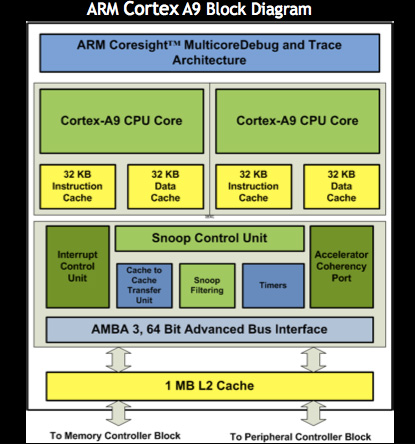
ARM11 was a single-issue, in-order architecture. Cortex A8 moved to dual-issue and A9 adds an out-of-order execution engine. The A9’s integer pipeline is also significantly shortened from 13 stages down to 9. The combination of out-of-order execution and a reduction in pipeline depth should give the Cortex A9 a healthy boost over the A8 at the same clock speed. The Cortex A8 is only supported in single-core configurations, while the Tegra 2 and TI’s OMAP 4 both use two A9 cores.
Each jump (ARM11 to A8 to A9) is good for at least a generational performance improvement (think 486 to Pentium, Pentium to Pentium Pro/II).
With each new generation of ARM architecture we also got a new manufacturing process and higher clock speeds. ARM11 was largely built at 90nm, while Cortex A8 started at 65nm. We saw most A8 SoCs transition to 40/45nm in 2010, which is where Cortex A9 will begin. The cadence will continue with A9 scaling down to 28nm in 2012 and the new Cortex A15 picking up where A9 leaves off.
Qualcomm’s Scorpion Core
The third contender in 2011 is Qualcomm’s Scorpion core. Scorpion is a dual-issue, mostly in-order microprocessor architecture developed entirely by Qualcomm. The Scorpion core implements the same ARMv7-A instruction set as the Cortex A8 and A9, however the CPU is not based on ARM’s Cortex A8 or A9. This is the point many seem to be confused about. Despite high level similarities, the Scorpion core is not Qualcomm’s implementation of a Cortex A8. Qualcomm holds an ARM architecture license which allows it to produce microprocessors that implement an ARM instruction set. This is akin to AMD holding an x86 license that allows it to produce microprocessors that are binary compatible with Intel CPUs. However calling AMD’s Phenom II a version of Intel’s Core i7 would be incorrect. Just like calling Scorpion a Cortex A8 is incorrect.
I mention high level similarities between Scorpion and the Cortex A8 simply because the two architectures appear alike. They both have dual-issue front ends and a 13-stage integer pipeline. Qualcomm claims the Scorpion core supports some amount of instruction reordering, however it’s not clear to what extent the CPU is capable of out-of-order execution. Intel’s Atom for example can reorder around certain instructions however it is far from an out-of-order CPU.
| Architecture Comparison | |||||||
| ARM11 | ARM Cortex A8 | ARM Cortex A9 | Qualcomm Scorpion | ||||
| Issue Width | single-issue | dual-issue | dual-issue | dual-issue | |||
| Pipeline Depth | 8 stages | 13 stages | 9 stages | 13 stages | |||
| Out of Order Execution | N | N | Y | Partial | |||
| FPU | Optional VFPv2 (not-pipelined) | VFPv3 (not-pipelined) | Optional VFPv3-D16 (pipelined) | VFPv3 (pipelined) | |||
| NEON | N/A | Y (64-bit wide) | Optional MPE (64-bit wide) | Y (128-bit wide) | |||
| Process Technology | 90nm | 65nm/45nm | 40nm | 40nm | |||
| Typical Clock Speeds | 412MHz | 600MHz/1GHz | 1GHz | 1GHz | |||
Scorpion has some big advantages on the floating point side. Qualcomm implements ARM’s VFPv3 vector floating point instruction set on Scorpion, the same instructions supported by the Cortex A8. The Cortex A8’s FPU wasn’t pipelined. A single instruction had to make it through the FP pipeline before the next instruction could be issued. For those of you who remember desktop processors, the Cortex A8’s non-pipelined FPU is reminiscent of Intel’s 486 and AMD’s K6. It wasn’t until the Pentium processor that Intel gained a pipelined FPU, and for AMD that came with the Athlon. As a result, floating point code runs rather slowly on the Cortex A8. You can get around the A8’s poor FP performance for some workloads by using NEON, which is a much higher performance SIMD engine paired with the Cortex A8.
The Scorpion’s VFPv3 FPU is fully pipelined. As a result, floating point performance is much improved. Qualcomm also implements support for NEON, but with a wider 128-bit datapath (compared to 64-bit in the A8 and A9). As a result, Qualcomm should have much higher VFP and NEON performance than the Cortex A8 (we see a good example of this in our Linpack performance results).
While all Cortex A8 designs incorporated ARM’s NEON SIMD engine, A9 gives you the option of integrating either a SIMD engine (ARM’s Media Processing Engine, aka NEON) or a non-vector floating point unit (VFPv3-D16). NVIDIA chose not to include the A9’s MPE and instead opted for the FPU. Unlike the A8’s FPU, in the A9 the FPU is fully pipelined—so performance is much improved. The A9’s FPU however is still not as quick at math as the optional SIMD MPE.
| Minimum Instruction Latencies (Single Precision) | ||||||
| Instruction | FADD | FSUB | FMUL | FMAC | ||
| ARM Cortex A8 (FPU) | 9 cycles | 9 cycles | 10 cycles | 18 cycles | ||
| ARM Cortex A9 (FPU) | 4 cycles | 4 cycles | 5 cycles | 8 cycles | ||
| ARM Cortex A8 (NEON) | 5 cycles | 5 cycles | 5 cycles | 9 cycles | ||
| ARM Cortex A9 (MPE/NEON) | 5 cycles | 5 cycles | 5 cycles | 9 cycles | ||
Remember that the A8's FPU isn't pipelined so it can't complete these instructions every cycle, resulting throughput that's nearly equal to the instruction latency. The A9's FPU by comparison is fully pipelined, giving it much higher instruction throughput compared to the A8.
NVIDIA claims implementing MPE would incur a 30% die penalty for a performance improvement that impacts only a minimal amount of code. It admits that at some point integrating a SIMD engine makes sense, just not yet. The table above shows a comparison of instruction latency on various floating point and SIMD engines in A8 and A9. TI’s OMAP 4 on the other hand will integrate ARM’s Cortex A9 MPE. Depending on the code being run, OMAP 4 could have a significant performance advantage vs. the Tegra 2. Qualcomm's FPU/NEON performance should remain class leading in non-bandwidth constrained applications.
Unfortunately for Qualcomm, much of what impacts smartphone application performance today isn’t bound by floating point performance. Future apps and workloads will definitely appreciate Qualcomm’s attention to detail, but loading a web page won’t touch the FPU.
The Scorpion core remains largely unchanged between SoC generations. It won’t be until 28nm in 2012 that Qualcomm introduces a new microprocessor architecture. Remember that as an architecture licensee Qualcomm is going to want to create architectures that last as long as possible in order to recover its initial investment. Microprocessor licensees however have less invested into each generation and can move to new architectures much faster.
Cache & Memory Controller Comparison
NVIDIA outfits the Tegra 2 with a 1MB L2 cache shared between the two Cortex A9 cores. A shared L2/private L1 structure makes the most sense for a dual-core CPU as we’ve learned from following desktop CPUs for years. It’s only once you make the transition to 3 or 4 cores that it makes sense to have private L2s and introduce a large, catch-all shared L3 cache.
Qualcomm’s upcoming QSD8660 only has a 512KB L2 cache shared between its two cores, while TI’s OMAP 4 has a Tegra 2-like 1MB L2. In these low power parts, having a large L2 with a good hit rate is very important. Moving data around a chip is always very power intensive. The close proximity of the L2 cache to the CPU cores helps keep power consumption down. Any data that has to be fetched from main memory requires waking up the external memory interface as well as the external or on-package DRAMs. A trip to main memory easily requires an order of magnitude more power than pulling data from a local cache.
While the OMAP 4 and Tegra 2 both have a larger L2 cache, it’s unclear what frequency the cache operates at. Qualcomm’s L2 operates at core frequency and as a result could offer higher bandwidth/lower latency operation.
NVIDIA opted for a single-channel 32-bit LPDDR2 memory interface. Qualcomm’s QSD8660/MSM8x60 and TI’s upcoming OMAP 4 have two LPDDR2 channels. NVIDIA claims that a narrower memory bus with more efficient arbitration logic is the best balance for power/performance at the 40nm process node. In order to feed the data hungry CPUs and GPU, NVIDIA specs the Tegra 2 for use with 600MHz datarate LPDDR2 memory (although the LG Optimus 2X actually has 800MHz datarate DRAM on package, it still only runs at 600MHz).
Assuming all memory controllers are equally efficient (which is an incorrect assumption), NVIDIA should have half the bandwidth of TI’s OMAP 4. NVIDIA’s larger L2 cache gives it an advantage over the QSD8660, giving Tegra 2 an effective memory latency advantage for a percentage of memory requests. Depending on the operating frequency of NVIDIA’s L2, Qualcomm could have a cache bandwidth advantage. The take away point here is that there’s no clear winner in this battle of specifications, just a comparison of tradeoffs.
The Dual-Core Comparison in 2011
In 2011 Qualcomm will introduce the QSD8660, a Snapdragon SoC with two 45nm Scorpion cores running at 1.2GHz. With a deeper pipeline, smaller cache and a largely in-order architecture, the QSD8660 should still trail NVIDIA’s Cortex A9 based Tegra 2 at the same clock speed. However Tegra 2 launches at 1GHz and it won’t be until Tegra 2 3D that we see 1.2GHz parts. Depending on timing we could see dual-core Qualcomm phones running at 1.2GHz competing with dual-core NVIDIA phones running at 1.0GHz. The winner between those two may not be as clear—it’ll likely vary based on workload.
At 1.2GHz I’d expect the Tegra 2 3D to be the fastest SoC for the entirety of 2011. Once 2012 rolls around we’ll reset the clock as Qualcomm introduces its next-generation microprocessor architecture.
NVIDIA clearly has an execution advantage as it is the first SoC maker to ship an ARM Cortex A9. NVIDIA’s biggest weakness on the CPU side is the lack of NEON support in Tegra 2, something that doesn’t appear to be an issue today but could be a problem in the future depending on how widespread NEON code becomes in apps. TI’s OMAP 4 includes both a NEON unit and a wider memory bus, the latter could be a performance advantage depending on how well designed the memory controller is.
Qualcomm is a bit behind on the architecture side. The Scorpion core began shipping in Snapdragon SoCs at the end of 2008 and the architecture won’t be refreshed until late 2011/2012. As Intel discovered with NetBurst, 4—5 year runs for a single microprocessor architecture are generally too long. Luckily Qualcomm appears to be on a ~3 year cadence at this point.
The QSD8660 running at 1.2GHz should be sufficient to at least keep Qualcomm competitive until the Scorpion’s replacement arrives (although I suspect NVIDIA/TI will take the crown with their A9 designs). One aspect we haven’t talked about (mostly because there isn’t any good data available) is power consumption. It’s unclear how the Scorpion core compares to the Cortex A9 in terms of power consumption at the same process node.


75 Comments
View All Comments
Exophase - Monday, February 7, 2011 - link
Thanks Anand.I'm surprised to hear that shot was from IMG, given that it was an IMG employee who made the comment originally about Tegra's 16-bit banding being evident on it, from the screenshot. Whoops. I do wonder what could be causing this, then.
Nonetheless, while that definitely makes my 16bit color claim invalid the depth buffer one should still hold. We might need to wait and see how much of a difference this actually makes, or rather how effective nVidia's 16-bit depth space is.
I'm glad to hear that you're as concerned about benchmarks on Android as I am. It's especially frustrating when I see people using them to try to indicate Atom being substantially better clock for clock than Cortex-A9.
Exophase - Monday, February 7, 2011 - link
Managed to miss this:"The test ramps from around 3k vertices to 15k vertices per frame, and 190k to 250k triangles per frame"
That line doesn't make any sense. How would you have hundreds of times more triangles than vertices? You must have meant something else.
sid1712 - Monday, February 7, 2011 - link
Great review as usual but i'm disappointed about the lack of details on the Sound Quality of the phone. A comparison of the sound quality (via headphone jack) alongside the iPhone 4 and the Galaxy S (with Voodoo kernel preferrably) would give a good idea about the SQ of the phone.ScentedKandle - Monday, February 7, 2011 - link
Related to this, the audio codec lists "lossless" but doesn't mention what format. Can the audio chip natively decode FLAC?teldar - Monday, February 7, 2011 - link
The order of buttons if the same as my droid x.Pjotr - Monday, February 7, 2011 - link
Does it really record 1920x1088? Does this unorthodox resolution play well on TVs, if you put it on a USB stick, for example?Brian Klug - Monday, February 7, 2011 - link
It plays back from the phone properly, and most of the playback software just does a crop. A ton of devices actually produce 1088 and don't make note of it, it should playback fine.-Brian
unmesh - Monday, February 7, 2011 - link
For active aka switching transistor power consumption, C*V^2*f (C is capacitance and f is frequency) is a better proxy than V^2/R.The conclusion that operating voltage has a huge effect remains the same.
Kevin098 - Monday, February 7, 2011 - link
Hey, can you make a video comparison between the iphone 4 retina display and Optimus 2x ?StormyParis - Monday, February 7, 2011 - link
Pages and pages of (apparently not very acurate, too) perf data, and not even one line on sound quality, which is one of my key buying points for a phone.No info on whether I'll be able to stream PC-resolution videos off my server to my bed over wifi.
Overall, not a very useful review. More like a dick size contest.