AMD's Radeon HD 6970 & Radeon HD 6950: Paving The Future For AMD
by Ryan Smith on December 15, 2010 12:01 AM ESTAdvancing Primitives: Dual Graphics Engines & New ROPs
AMD has clearly taken NVIDIA’s comments on geometry performance to heart. Along with issuing their manifesto with the 6800 series, they’ve also been working on their own improvements for their geometry performance. As a result AMD’s fixed function Graphics Engine block is seeing some major improvements for Cayman.
Prior to Cypress, AMD had 1 graphics engine, which contained 1 each of the fundamental blocks: the rasterizers/hierarchical-Z units, the geometry/vertex assemblers, and the tessellator. With Cypress AMD added a 2nd rasterizer and 2nd hierarchical-Z unit, allowing them to set up 32 pixels per clock as opposed to 16 pixels per clock. However while AMD doubled part of the graphics engine, they did not double the entirety of it, meaning their primitive throughput rate was still 1 primitive/clock, a typical throughput rate even at the time.
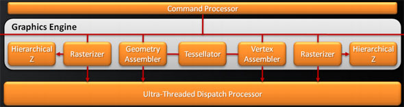
Cypress's Graphics Engine
In 2010 with the launch of Fermi, NVIDIA raised the bar on primitive performance, with rasterization moved to NVIDIA’s GPCs, NVIDIA could theoretically push out as many primitives/clock as they had GPCs, in the case of GF100/GF110 pushing this to 4 primitives/clock, a simply massive improvement in geometry performance for a single generation.
With Cayman AMD is catching up with NVIDIA by increasing their own primitive throughput rate, though not by as much as NVIDIA did with Fermi. For Cayman the rest of the graphics engine is being fully duplicated – Cayman will have 2 separate graphics engines, each containing one fundamental block, and each capable of pushing out 1 primitive/clock. Between the two of them AMD’s maximum primitive throughput rate will now be 2 primitives/clock; half as much as NVIDIA but twice that of Cypress.
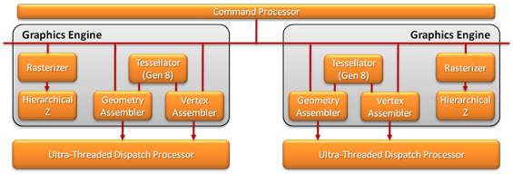
Cayman's Dual Graphics Engines
As was the case for NVIDIA, splitting up rasterization and tessellation is not a straightforward and easy task. For AMD this meant teaching the graphics engine how to do tile-based load balancing so that the workload being spread among the graphics engines is being kept as balanced as possible. Furthermore AMD believes they have an edge on NVIDIA when it comes to design - AMD can scale the number of eraphics engines at will, whereas NVIDIA has to work within the logical confines of their GPC/SM/SP ratios. This tidbit would seem to be particularly important for future products, when AMD looks to scale beyond 2 graphics engines.
At the end of the day all of this tinking with the graphics engines is necessary in order for AMD to further improve their tessellation performance. AMD’s 7th generation tessellator improved their performance at lower tessellation factors where the tessellator was the bottleneck, but at higher tessellation factors the graphics engine itself is the bottleneck as the graphics engine gets swamped with more incoming primitives than it can set up in a single clock. By having two graphics engines and a 2-primitive/clock rasterization rate, AMD is shifting the burden back away from the graphics engine.
Just having two 7th generation-like tessellators goes a long way towards improving AMD’s tessellation performance. However all of that geometry can still lead to a bottleneck at times, which means it needs to be stored somewhere until it can be processed. As AMD has not changed any cache sizes for Cayman, there’s the same amount of cache for potentially thrice as much geometry, so in order to keep things flowing that geometry has to go somewhere. That somewhere is the GPU’s RAM, or as AMD likes to put it, their “off-chip buffer.” Compared to cache access RAM is slow and hence this isn’t necessarily a desirable action, but it’s much, much better than stalling the pipeline entirely while the rasterizers clear out the backlog.
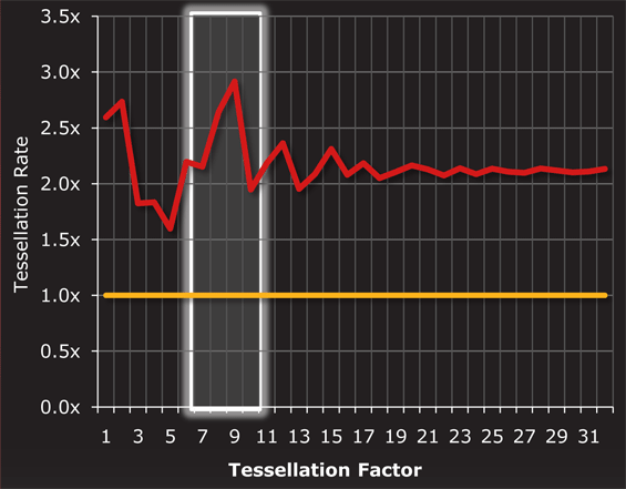
Red = 6970. Yellow = 5870
Overall, clock for clock tessellation performance is anywhere between 1.5x and 3x that of Cypress. In situations where AMD’s already improved tessellation performance at lower tessellation factors plays a part, AMD approaches 3x performance; while at around a factor of 5 the performance drops to near 1.5x. Elsewhere performance is around 2x that of Cypress, representing the doubling of graphics engines.
Tessellation also plays a factor in AMD’s other major gaming-related improvement: ROP performance. As tessellation produces many mini triangles, these triangles begin to choke the ROPs when performing MSAA. Although tessellation isn’t the only reason, it certainly plays a factor in AMD’s reasoning for improving their ROPs to improve MSAA performance.
The 32 ROPs (the same as Cypress) have been tweaked to speed up processing of certain types of values. In the case of both signed and unsigned normalized INT16s, these operations are now 2x faster. Meanwhile FP32 operations are now 2x to 4x faster depending on the scenario. Finally, similar to shader read ops for compute purposes, ROP write ops for graphics purposes can be coalesced, improving performance by requiring fewer operations.


168 Comments
View All Comments
versesuvius - Friday, December 17, 2010 - link
Ananke,I am not very knowledgeable about this, but I don't think a modern GPU can fit inside a CPU for now. A better idea would be a console on a card. The motherboards on the consoles are not much bigger than the large graphic cards of today. A console card for $100 would be great. I am sure that there is no technical obstacles that the average electronic wizard cannot overcome, doing that.
Sure, there is a use for everything. I can imagine that every single human being on earth can find a use for a Ferrari, but the point is that even those who do have it, do not use it as often as their other car, (Toyota, VW or whatever). In fact, there is rarely a Ferrari that has more than 20,000 km on it, and even that is put on it by successive owners, not one. The average total an ordinary person can stand a Ferrari is 5000 KM. (Disclaimer: I do not have one. I only read something to that effect somewhere). Having said that, I do have a sense of the "need for speed". I can remember sitting in front of the university's 80286 waiting for the FE program to spit out the results, one node at a time, click, click, ... . You have millions of polygons, we can have billions of mesh nodes, and that even does not even begin to model a running faucet. How's that for the need for speed. I do appreciate the current speeds. However, the CPU deal was and is a straight one. The graphic card deals, today, are not. To be clear, the "and" in "High End"s and "Fool"s is an inclusive one. "Someone will pay for it", was also initiated in the eighties of the last century. By the way, the big question "can it play crysis", will no longer be. Crysis 2 is coming to the consoles.
Quidam67 - Friday, December 17, 2010 - link
"But can it play Crysis" should be in the Urban dictionary as a satirical reference on graphics code that combines two potent attributes: 1) is way ahead of its time in terms of what current hardware can support 2) is so badly written and optimised that even hardware that should be able to run it still can't.In 1000 years time when Organic Graphics cards that you can plug into your head still can't run it smoothly @2560*1600 60fps they will realise the joke was on us and that the code itself was written to run more and more needless loops in order to overwhelm any amount of compute-resource thrown at it.
Iketh - Friday, December 24, 2010 - link
LOLmarc1000 - Friday, December 17, 2010 - link
I swear I've read ALL the comments to see if anyone already pointed it... but no one did.I feel a bit disappointed with this launch too (I have a 5770 and wanted to get 6950 but was wanting a bigger increase %-wise). But one thing interesting it the number of Stream Processors in the new gpus. By the "pure processor" count this number decreased from 1600 SPs on 5870 to 1536 SPs on 6970. But the size of the VLIW processors changed too. It was 5 SPs on 5870 and now is 4 SPs.
So we have:
hd5870 = 1600 SPs / 5 = 320 "processors"
hd6970 = 1536 SPs / 4 = 384 "processors"
if we take that 384 and multiply by 5, we would have 1920 SPs on the new generation (on par with many rumors). this is 20% more shaders. and considering AMD is saying that the new VLIW4 is 10% faster than VLIW5 we should have more than 20% increase in all situations. but this is only true in the minority of tests (like crysis at 2560x1660 where it is 24%, but in the same game at 1680x1050 the increase is only 16%). and at the same time the minimun FPS got better, yet in another games the difference is smaller.
but then again, I was expecting a little more. I believe the 6950 will be a worthy upgrade to me, but the expectations were so high that too much people ended a little disappointed... myself included.
Sunburn74 - Tuesday, December 28, 2010 - link
Well... at least they delivered on time and didn't make you wait 6 more months to simply deliver an equivalent, if not considerably worse, product.Mr Perfect - Friday, December 17, 2010 - link
Yes, the minimums are appreciated when they're included.It would be even better if the framerates was displayed as a line graph instead of a bar graph. That way readers could tell if an average consisted of a lot of high peaks and low valleys, or really was a nice smooth experience all the way through. Some other review sites use linegraphs and while I visit Anandtech for it's timeliness, professionalism, industry insight and community involvement, I go to the other sites for the actual performance numbers.
Quidam67 - Friday, December 17, 2010 - link
There is further rationale for splitting the article. Lets say someone is googling "HD 6970 architecture" perhaps they will pick up this review, or perhaps they won't, but either way, if they see that it is actually a review on the cards, they might be inclined to bypass it in favour of a more focused piece.And again, there is no reason why the Architecture Article can't provide a hyperlink to the review, if the reader then decides they want to see how that architecture translates into performance on the current generation of cards supporting it.
I really hope AT are reading this and giving it some consideration. As you say, they are a great sight and no one is disputing that, but it's not a religion, so you should be allowed to question it without being accused of blasphemy :O)
dustcrusher - Friday, December 17, 2010 - link
It really comes down to how important the mainstream market is. If they are a large enough segment of the market, one company using a simple, easy-to-grasp naming convention would likely grab some market share. Make it easy to buy your product and at least some people will be more likely to do so.If not, then it's fun to talk about but not terribly important. Tech-savvy folk will buy whatever meets their needs price/performance-wise after doing research, even if a card is named the Transylvania 6-9000 or the Wankermeister GTFO. Eager to please tech-naive folk are going to buy the largest model number they can get with the money they have, because "larger model numbers = bigger/better equipment" is a long-established consumer shorthand.
I have a half-baked idea for a model numbering system that's based around the key specs of the card- it's a 5 digit system where the first digit is the hardware platform ID (like what we have now, mostly) and the other four would represent combinations of other specs (one digit could be the lowest memory clock speed and bus width would be 1, the next lowest memory clock speed and lowest bus width would be 2, etc).
No idea if this could actually be implemented- there are probably too many variables with GPU/memory clock speeds, among other things.
Shinobi_III - Saturday, December 18, 2010 - link
If you ever saw Nvidia 4xAA in action, you know it's not as smooth as the radeon implementation (especially in motion) and z-buffer miscalculations has always been a nvidia feature.Go up a hill in Fallout New Vegas and look at Vegas in the horizon, with Nvidia cards it always looks like a disco due to meshes overlapping. Now do the same on Radeon.
TheUsual - Saturday, December 18, 2010 - link
Right now, Newegg has a 6870 for $200 after rebate. Two of these makes for an awesome value at $400. The top tier of cards doesn't give a corresponding increase in performance for the extra cost. Two 6950s costs 50% more but does not give you 50% more FPS. Two GTX 460 1GBs is also a great bang for the buck at $300.Neither of these lets you do triple SLI/XFIRE however. That would be what would be paying extra for.
My hope is that the price will drop on the 6950 by around February. By then the GTX 560 should be out and might drive prices down some. The benchmarks could change some with Sandy Bridge too, if they are currently CPU bound.