AMD's Radeon HD 6970 & Radeon HD 6950: Paving The Future For AMD
by Ryan Smith on December 15, 2010 12:01 AM ESTCayman: The Last 32nm Castaway
With the launch of the Barts GPU and the 6800 series, we touched on the fact that AMD was counting on the 32nm process to give them a half-node shrink to take them in to 2011. When TSMC fell behind schedule on the 40nm process, and then the 32nm process before canceling it outright, AMD had to start moving on plans for a new generation of 40nm products instead.
The 32nm predecessor of Barts was among the earlier projects to be sent to 40nm. This was due to the fact that before 32nm was even canceled, TSMC’s pricing was going to make 32nm more expensive per transistor than 40nm, a problem for a mid-range part where AMD has specific margins they’d like to hit. Had Barts been made on the 32nm process as projected, it would have been more expensive to make than on the 40nm process, even though the 32nm version would be smaller. Thus 32nm was uneconomical for gaming GPUs, and Barts was moved to the 40nm process.
Cayman on the other hand was going to be a high-end part. Certainly being uneconomical is undesirable, but high-end parts carry high margins, especially if they can be sold in the professional market as compute products (just ask NVIDIA). As such, while Barts went to 40nm, Cayman’s predecessor stayed on the 32nm process until the very end. The Cayman team did begin planning to move back to 40nm before TSMC officially canceled the 32nm process, but if AMD had a choice at the time they would have rather had Cayman on the 32nm process.
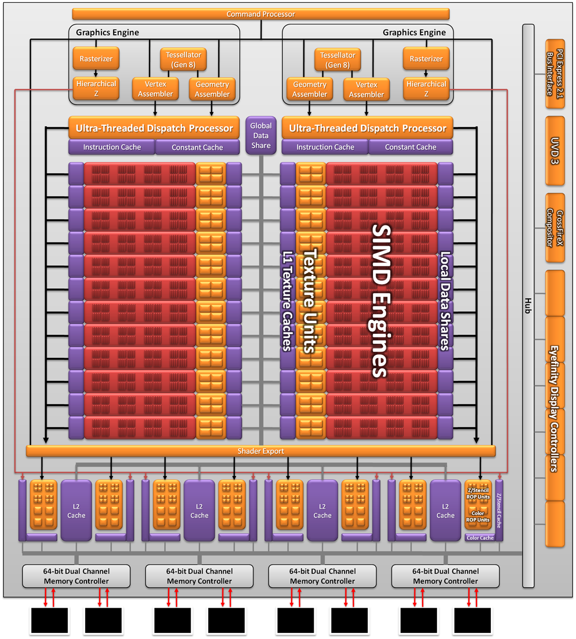
As a result the Cayman we’re seeing today is not what AMD originally envisioned as a 32nm part. AMD won’t tell us everything that they had to give up to create the 40nm Cayman (there has to be a few surprises for 28nm) but we do know a few things. First and foremost was size; AMD’s small die strategy is not dead, but getting the boot from the 32nm process does take the wind out of it. At 389mm2 Cayman is the largest AMD GPU since the disastrous R600, and well off the sub-300mm2 size that the small die strategy dictates. In terms of efficient usage of space though AMD is doing quite well; Cayman has 2.64 billion transistors, 500mil more than Cypress. AMD was able to pack 29% more transistors in only 16% more space.
Even then, just reaching that die size is a compromise between features and production costs. AMD didn’t simply settle for a larger GPU, but they had to give up some things to keep it from being even larger. SIMDs were on the chopping block; 32nm Cayman would have had more SIMDs for more performance. Features were also lost, and this is where AMD is keeping mum. We know PCI Express 3.0 functionality was scheduled for the 32nm part, where AMD had to give up their PCIe 3.0 controller for a smaller 2.1 controller to make up for their die size difference. This in all honesty may have worked out better for them: PCIe 3.0 ended up being delayed until November, so suitable motherboards are still at least months away.
The end result is that Cayman as we know it is a compromise to make it happen on 40nm. AMD got their new VLIW4 architecture, but they had to give up performance and an unknown number of features to get there. On the flip side this will make 28nm all the more interesting, as we’ll get to see many of the features that were supposed to make it for 2010 but never arrived.


168 Comments
View All Comments
versesuvius - Friday, December 17, 2010 - link
Ananke,I am not very knowledgeable about this, but I don't think a modern GPU can fit inside a CPU for now. A better idea would be a console on a card. The motherboards on the consoles are not much bigger than the large graphic cards of today. A console card for $100 would be great. I am sure that there is no technical obstacles that the average electronic wizard cannot overcome, doing that.
Sure, there is a use for everything. I can imagine that every single human being on earth can find a use for a Ferrari, but the point is that even those who do have it, do not use it as often as their other car, (Toyota, VW or whatever). In fact, there is rarely a Ferrari that has more than 20,000 km on it, and even that is put on it by successive owners, not one. The average total an ordinary person can stand a Ferrari is 5000 KM. (Disclaimer: I do not have one. I only read something to that effect somewhere). Having said that, I do have a sense of the "need for speed". I can remember sitting in front of the university's 80286 waiting for the FE program to spit out the results, one node at a time, click, click, ... . You have millions of polygons, we can have billions of mesh nodes, and that even does not even begin to model a running faucet. How's that for the need for speed. I do appreciate the current speeds. However, the CPU deal was and is a straight one. The graphic card deals, today, are not. To be clear, the "and" in "High End"s and "Fool"s is an inclusive one. "Someone will pay for it", was also initiated in the eighties of the last century. By the way, the big question "can it play crysis", will no longer be. Crysis 2 is coming to the consoles.
Quidam67 - Friday, December 17, 2010 - link
"But can it play Crysis" should be in the Urban dictionary as a satirical reference on graphics code that combines two potent attributes: 1) is way ahead of its time in terms of what current hardware can support 2) is so badly written and optimised that even hardware that should be able to run it still can't.In 1000 years time when Organic Graphics cards that you can plug into your head still can't run it smoothly @2560*1600 60fps they will realise the joke was on us and that the code itself was written to run more and more needless loops in order to overwhelm any amount of compute-resource thrown at it.
Iketh - Friday, December 24, 2010 - link
LOLmarc1000 - Friday, December 17, 2010 - link
I swear I've read ALL the comments to see if anyone already pointed it... but no one did.I feel a bit disappointed with this launch too (I have a 5770 and wanted to get 6950 but was wanting a bigger increase %-wise). But one thing interesting it the number of Stream Processors in the new gpus. By the "pure processor" count this number decreased from 1600 SPs on 5870 to 1536 SPs on 6970. But the size of the VLIW processors changed too. It was 5 SPs on 5870 and now is 4 SPs.
So we have:
hd5870 = 1600 SPs / 5 = 320 "processors"
hd6970 = 1536 SPs / 4 = 384 "processors"
if we take that 384 and multiply by 5, we would have 1920 SPs on the new generation (on par with many rumors). this is 20% more shaders. and considering AMD is saying that the new VLIW4 is 10% faster than VLIW5 we should have more than 20% increase in all situations. but this is only true in the minority of tests (like crysis at 2560x1660 where it is 24%, but in the same game at 1680x1050 the increase is only 16%). and at the same time the minimun FPS got better, yet in another games the difference is smaller.
but then again, I was expecting a little more. I believe the 6950 will be a worthy upgrade to me, but the expectations were so high that too much people ended a little disappointed... myself included.
Sunburn74 - Tuesday, December 28, 2010 - link
Well... at least they delivered on time and didn't make you wait 6 more months to simply deliver an equivalent, if not considerably worse, product.Mr Perfect - Friday, December 17, 2010 - link
Yes, the minimums are appreciated when they're included.It would be even better if the framerates was displayed as a line graph instead of a bar graph. That way readers could tell if an average consisted of a lot of high peaks and low valleys, or really was a nice smooth experience all the way through. Some other review sites use linegraphs and while I visit Anandtech for it's timeliness, professionalism, industry insight and community involvement, I go to the other sites for the actual performance numbers.
Quidam67 - Friday, December 17, 2010 - link
There is further rationale for splitting the article. Lets say someone is googling "HD 6970 architecture" perhaps they will pick up this review, or perhaps they won't, but either way, if they see that it is actually a review on the cards, they might be inclined to bypass it in favour of a more focused piece.And again, there is no reason why the Architecture Article can't provide a hyperlink to the review, if the reader then decides they want to see how that architecture translates into performance on the current generation of cards supporting it.
I really hope AT are reading this and giving it some consideration. As you say, they are a great sight and no one is disputing that, but it's not a religion, so you should be allowed to question it without being accused of blasphemy :O)
dustcrusher - Friday, December 17, 2010 - link
It really comes down to how important the mainstream market is. If they are a large enough segment of the market, one company using a simple, easy-to-grasp naming convention would likely grab some market share. Make it easy to buy your product and at least some people will be more likely to do so.If not, then it's fun to talk about but not terribly important. Tech-savvy folk will buy whatever meets their needs price/performance-wise after doing research, even if a card is named the Transylvania 6-9000 or the Wankermeister GTFO. Eager to please tech-naive folk are going to buy the largest model number they can get with the money they have, because "larger model numbers = bigger/better equipment" is a long-established consumer shorthand.
I have a half-baked idea for a model numbering system that's based around the key specs of the card- it's a 5 digit system where the first digit is the hardware platform ID (like what we have now, mostly) and the other four would represent combinations of other specs (one digit could be the lowest memory clock speed and bus width would be 1, the next lowest memory clock speed and lowest bus width would be 2, etc).
No idea if this could actually be implemented- there are probably too many variables with GPU/memory clock speeds, among other things.
Shinobi_III - Saturday, December 18, 2010 - link
If you ever saw Nvidia 4xAA in action, you know it's not as smooth as the radeon implementation (especially in motion) and z-buffer miscalculations has always been a nvidia feature.Go up a hill in Fallout New Vegas and look at Vegas in the horizon, with Nvidia cards it always looks like a disco due to meshes overlapping. Now do the same on Radeon.
TheUsual - Saturday, December 18, 2010 - link
Right now, Newegg has a 6870 for $200 after rebate. Two of these makes for an awesome value at $400. The top tier of cards doesn't give a corresponding increase in performance for the extra cost. Two 6950s costs 50% more but does not give you 50% more FPS. Two GTX 460 1GBs is also a great bang for the buck at $300.Neither of these lets you do triple SLI/XFIRE however. That would be what would be paying extra for.
My hope is that the price will drop on the 6950 by around February. By then the GTX 560 should be out and might drive prices down some. The benchmarks could change some with Sandy Bridge too, if they are currently CPU bound.