AMD's Radeon HD 6970 & Radeon HD 6950: Paving The Future For AMD
by Ryan Smith on December 15, 2010 12:01 AM ESTVLIW4: Finding the Balance Between TLP, ILP, and Everything Else
To properly frame why AMD went with a VLIW4 design we’d have to first explain why AMD went with a VLIW5 design. And to do that we’d have to go back even further to the days of DirectX 9, and thus that is where we will start.
Back in the days of yore, when shading was new and pixel and vertex shaders were still separate entities, AMD (née ATI) settled on a VLIW5 design for their vertex shaders. Based on their data this was deemed the ideal configuration for a vertex shader block, as it allowed them to process a 4 component dot product (e.g. w, x, y, z) and a scalar component (e.g. lighting) at the same time.
Fast forward to 2007 and the introduction of AMD’s Radeon HD 2000 series (R600), where AMD introduced their first unified architecture for the PC. AMD went with a VLIW5 design once more, as even though the product was their first DX10 product it still made sense to build something that could optimally handle DX9 vertex shaders. This was also well before GPGPU had a significant impact on the market, as AMD had at best toyed around with the idea late in the X1K series’ lifetime (and well after R600 was started).
Now let us jump to 2008, when Cayman’s predecessors were being drawn up. GPGPU computing is still fairly new – NVIDIA is at the forefront of a market that only amounts to a few million dollars at best – and DX10 games are still relatively rare. With 2+ years to bring up a GPU, AMD has to be looking forward at where things will be in 2010. Their predictions are that GPGPU computing will finally become important, and that DX9 games will fade in importance to DX10/11 games. It’s time to reevaluate VLIW5.
This brings us to the present day and the launch of Cayman. GPGPU computing is taking off, and DX10 & DX11 alongside Windows 7 are gaining momentum while DX9 is well past its peak. AMD’s own internal database of games tells them an interesting story: the average slot utilization is 3.4 – on average a 5th streaming processor is going unused in games. VLIW5, which made so much sense for DX9 vertex shaders is now becoming too wide, while scalar and narrow workloads are increasing in number. The stage is set for a narrower Streaming Processor Unit; enter VLIW4.
As you may recall from a number of our discussions on AMD’s core architecture, AMD’s architecture is heavily invested in Instruction Level Parallelism, that is having instructions in a single thread that have no dependencies on each other that can be executed in parallel. With VLIW5 the best case scenario is that 5 instructions can be scheduled together on every SPU every clock, a scenario that rarely happens. We’ve already touched on how in games AMD is seeing an average of 3.4, which is actually pretty good but still is under 80% efficient. Ultimately extracting ILP from a workload is hard, leading to a wide delta between the best and worst case scenarios.
Meanwhile all of this is in stark contrast to Thread Level Parallelism (TLP), which looks for threads that can be run at the same time without having any interdependencies. This is where NVIDIA has focused their energies at the high-end, as GF100/GF100 are both scalar architectures that rely on TLP to achieve efficient operation.
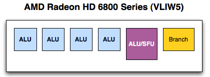
Ultimately the realization is that AMD’s VLIW5 architecture is not the best architecture going forward. Up until now it has made sense at a high efficiency gaming-oriented design, and even today in a gaming part like the 6800 series it’s still a reasonable choice. But AMD needs a new architecture for the future, not only as something that’s going to better fit their 3.4 shader average, but something that is better designed for compute workloads. AMD’s choice is an overhauled version of their existing architecture. Overall it’s built on a solid foundation, but VLIW5 is too wide to meet their future goals.
The solution is to shrink their VLIW5 SPU to a VLIW4 SPU. Specifically, the solution is to remove the t-unit, the architecture’s 5th SP and largest SP that’s capable of both regular INT/FP operations as well as being responsible for transcendental operations. In the case of regular INT/FP operations this means an SPU is reduced from being able to process 5 operations at once to 4. While in the case of transcendentals an SPU now ties together 3 SPs to process 1 transcendental in the same period of time, representing a much more severe reduction in theoretical performance as an SPU can only process 1 transcendental + 1 INT/FP per clock as opposed to 1 transcendental + 4 INT/FP operations (or any variations).
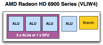
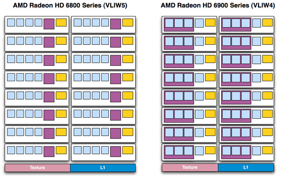
There are a number of advantages to this change. As far as compute is concerned, the biggest advantage is that much of the space previously allocated to the t-unit can now be scrounged up to build more SIMDs. Cypress had 20 SIMDs while Cayman has 24; on average Cayman’s shader block is 10% more efficient per mm2 than Cypress’s , taking in to account the fact that Cayman’s SPs are a bit larger than Cypress’ to pick up the workload the t-unit would handle. The SIMDs are further tied to a number of attributes: the number of texture units, the number of threads that can be in flight at once, and the number of FP64 operations that can be completed per clock. The latter is particularly important for AMD’s compute efforts, as they can now retire FP64 FMA/MUL operations at 1/4th their FP32 rate, in the case of a full Cayman up to 384/clock. Technically speaking they’re no faster per SPU, but with this layout change they have more SPUs to work with, improving their performance.
Fewer SPs per SIMD = More Space For More SIMDs
There are even ancillary benefits within the individual SPUs. While the SP count changed the register file did not, leading to less pressure on each SPU’s registers as now only 4 SPs vie for register space. Even scheduling is easier as there are fewer SPs to schedule and the fact that they’re all alike means the scheduler no longer has to take into consideration the difference between the w/x/y/z units and the t-unit.
Meanwhile in terms of gaming the benefits are similar. Games that were already failing to fully utilize the VLIW5 design now have additional SIMDs to take advantage of, and as rendering is still an embarrassingly parallel operation as far as threading is concerned, it’s very easy to further divide the rendering workload in to more threads to take advantage of this change. The extra SIMDs mean that Cayman has additional texturing horsepower over Cypress, and the overall compute:texture ratio has been reduced, a beneficial situation for any games that are texture/filtering bound more than they’re compute bound.
Of course any architectural change involves tradeoffs, so it’s not a pure improvement. For gaming the tradeoff is that Cayman isn’t going to be well suited to VLIW5-style vertex shaders; generally speaking games using such shaders already run incredibly fast, but if they’re even GPU-bound in the first place they’re not going to gain much from Cayman. The other big tradeoff is when transcendental operations are paired with vector operations, as Cypress could handle both in one clock while Cayman will take two. It’s AMD’s belief that these operations are rare enough that the loss of performance in this one situation is worth it for the gain in performance everywhere else.
It’s worth noting that AMD still considers VLIW4 to be a risky/experimental design, or at least this is their rationale for going with it first on Cayman while sticking to VLIW5 elsewhere. At this point we’d imagine the real experiment to already be over, as AMD would already be well in the middle of designing Cayman’s 28nm successor, so they undoubtedly know if they’ll be using VLIW4 in the future.
Finally, the switch to a new VLIW architecture means the AMD driver team has to do some relearning. While VLIW4 is quite similar to VLIW5 it’s not by any means identical, which is both good and bad for performance purposes. The bad news is that it means many of AMD’s VLIW5-centric shader compiler tricks are no longer valid; at the start shader compiler performance is going to be worse while AMD learns how to better program a VLIW4 design. The good news is that in time they’re going to learn how to better program a VLIW4 design, meaning there’s the potential for sizable performance increases throughout the lifetime of the 6900 series. That doesn’t mean they’re guaranteed, but we certainly expect at least some improvement in shader performance as the months wear on.
On that note these VLIW changes do mean that some code is going to have to be rewritten to better deal with the reduction of VLIW width. AMD’s shader compiler goes through a number of steps to try to optimize code, but if kernels were written specifically to organize instructions to go through AMD’s shaders in a 5-wide fashion, then there’s only so much AMD’s compiler can do. Of course code doesn’t have to be written that way, but it is the best way to maximize ILP and hence shader performance.
VLIW5:
- 4 32-bit FP MAD
- Or 2 64-bit FP MUL or ADD
- Or 1 64-bit FP MAD
- Or 4 24-bit Int MUL or ADD
- Plus 1 transcendental or 1 32-bit FP MAD
VLIW4:
- 4 32-bit FP MAD/MUL/ADD
- Or 2 64-bit FP ADD
- Or 1 64-bit FP MAD/FMA/MUL
- Or 4 24-bit INT MAD/MUL/ADD
- Or 4 32-bit INT ADD/Bitwise
- Or 1 32-bit MAD/MUL
- Or 1 64-bit ADD
- Or 1 transcendental plus 1 32-bit FP MAD


168 Comments
View All Comments
B3an - Thursday, December 16, 2010 - link
Very stupid uninformed and narrow-minded comment. People like you never look to the future which anyone should do when buying a graphics card, and you completely lack any imagination. Theres already tons of uses for GPU computing, many of which the average computer user can make use of, even if it's simply encoding a video faster. And it will be use a LOT more in the future.Most people, especially ones that game, dont even have 17" monitors these days. The average size monitor for any new computer is at least 21" with 1680 res these days. Your whole comment is as if everyone has the exact same needs as YOU. You might be happy with your ridiculously small monitor, and playing games at low res on lower settings, and it might get the job done, but lots of people dont want this, they have standards and large monitors and needs to make use of these new GPU's. I cant exactly see many people buying these cards with a 17" monitor!
CeepieGeepie - Thursday, December 16, 2010 - link
Hi Ryan,First, thanks for the review. I really appreciate the detail and depth on the architecture and compute capabilities.
I wondered if you had considered using some of the GPU benchmarking suites from the academic community to give even more depth for compute capability comparisons. Both SHOC (http://ft.ornl.gov/doku/shoc/start) and Rodinia (https://www.cs.virginia.edu/~skadron/wiki/rodinia/... look like they might provide a very interesting set of benchmarks.
Ryan Smith - Thursday, December 16, 2010 - link
Hi Ceepie;I've looked in to SHOC before. Unfortunately it's *nix-only, which means we can't integrate it in to our Windows-based testing environment. NVIDIA and AMD both work first and foremost on Windows drivers for their gaming card launches, so we rarely (if ever) have Linux drivers available for the launch.
As for Rodinia, this is the first time I've seen it. But it looks like their OpenCL codepath isn't done, which means it isn't suitable for cross-vendor comparisons right now.
IdBuRnS - Thursday, December 16, 2010 - link
"So with that in mind a $370 launch price is neither aggressive nor overpriced. Launching at $20 over the GTX 570 isn’t going to start a price war, but it’s also not so expensive to rule the card out. "At NewEgg right now:
Cheapest GTX 570 - $509
Cheapest 6970 - $369
$30 difference? What are you smoking? Try $140 difference.
IdBuRnS - Thursday, December 16, 2010 - link
Oops, $20 difference. Even worse.IdBuRnS - Thursday, December 16, 2010 - link
570...not 580.../hangsheadinshame
epyon96 - Thursday, December 16, 2010 - link
This was a very interesting discussion to me in the article.I'm curious if Anandtech might expand on this further in a future dedicated article comparing what NVIDIA is using to AMD.
Are they also more similar to VLIW4 or VLIW5?
Can someone else shed some light on it?
Ryan Smith - Thursday, December 16, 2010 - link
We wrote something almost exactly like you're asking for for our Radeon HD 4870 review.http://www.anandtech.com/show/2556
AMD and NVIDIA's compute architectures are still fundamentally the same, so just about everything in that article still holds true. The biggest break is VLIW4 for the 6900 series, which we covered in our article this week.
But to quickly answer your question, GF100/GF110 do not immediately compare to VLIW4 or VLIW5. NVIDIA is using a pure scalar architecture, which has a number of fundamental differences from any VLIW architecture.
dustcrusher - Thursday, December 16, 2010 - link
The cheap insults are nothing but a detriment to what is otherwise an interesting argument, even if I don't agree with you.As far as the intellect of Anandtech readers goes, this is one of the few sites where almost all of the comments are worth reading; most sites are the opposite- one or two tiny bits of gold in a big pan of mud.
I'm not going to "vastly overestimate" OR underestimate your intellect though- instead I'm going to assume that you got caught up in the moment. This isn't Tom's or Dailytech, a little snark is plenty.
Arnulf - Thursday, December 16, 2010 - link
When you launch an application (say a game), it is likely to be the only active thread running on the system, or perhaps one of very few active threads. CPU with Turbo function will clock up as high as possible to run this main thread. When further threads are launched by the application, CPU will inevitably increase its power consumption and consequently clock down.While CPU manufacturers don't advertise this functionality in this manner, it is really no different from PowerTune.
Would PowerTune technology make you feel any better if it was marketed the other way around, the way CPUs are ? (mentioning lowest frequencies and clock boost provided that thermal cap isn't met yet)