NVIDIA's GeForce GTX 580: Fermi Refined
by Ryan Smith on November 9, 2010 9:00 AM ESTMeet the GTX 580
Since we’ve already discussed the cooling, let’s dive right in to the rest of the GTX 580, shall we?
Launching today will be a single GTX 580 design, the reference design. Talking to our contacts, semi-custom designs (designs using the reference PCB with a different cooler) are due in the next few weeks assuming everything goes to plan and of course there’s ample supply. And while we’re on that note, NVIDIA let us know that with their focus on cooling on the GTX 580 they aren’t going to be letting custom GTX 580 designs go out without a more thorough inspection. The acoustic performance of the reference GTX 580 is going to be the bare minimum to get a design approved – if it can’t beat the reference design, NVIDIA won’t allow it. We consider this a matter of brand protection for the company, as a bad/loud GeForce is still a GeForce all the same.
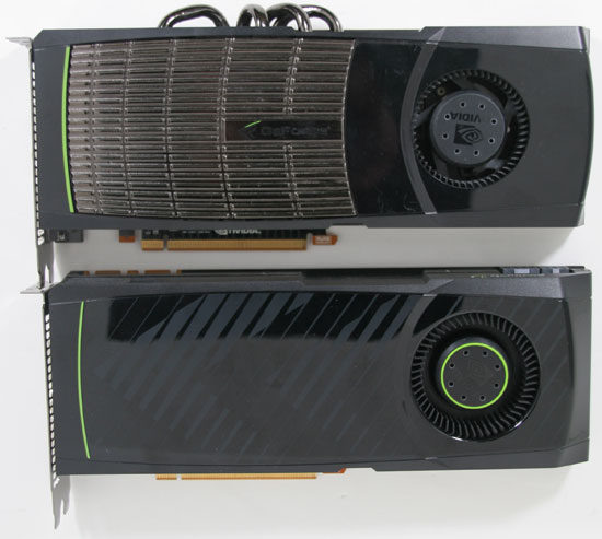
Top: GTX 480. Bottom: GTX580
With the reference design the resulting card is very close to being a GTX 285/480 hybrid. In terms of overall design it ends up looking very similar to the GTX 285. At 10.5” long it’s the same length as the GTX 480 or a smidge longer than the GTX 285, and should fit in to any cases those cards could work in. Power connectivity is the same as the GTX 480, with 6pin and 8pin PCIe sockets being located at the top of the card, providing easy access to the sockets. At 244W TDP the card draws too much for 6+6, but you can count on an eventual GTX 570 to fill that niche. Meanwhile NVIDIA has kept the 480’s detachable shroud lid, meaning you can remove the cover of the shroud without disturbing the rest of the card; it’s worth noting that it’s secured with screws rather than laches this time however.
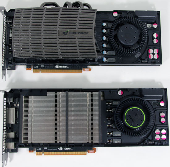
Heatsinks Exposed! Top: GTX 480. Bottom: GTX 580
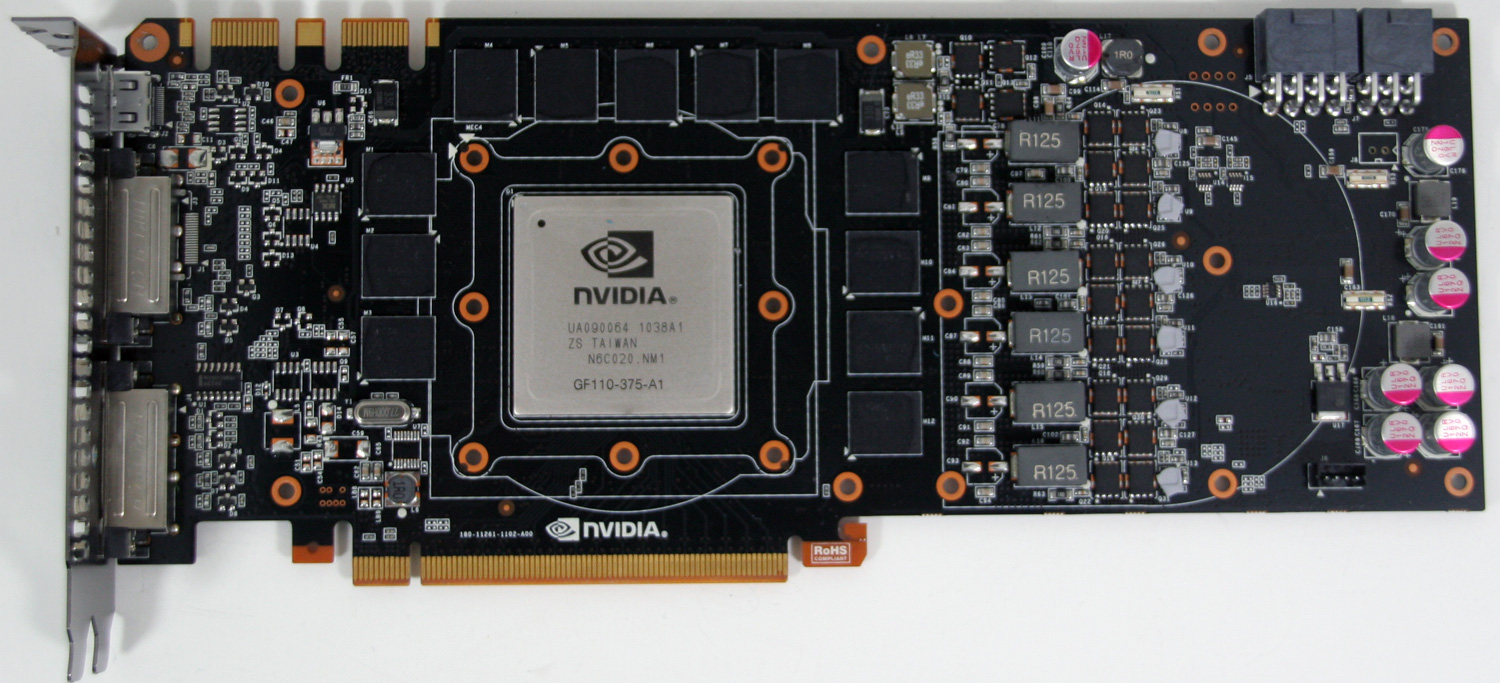
On the front side of the PCB you’ll find the 12 GDDR5 chips composing the card’s 384bit memory bus. The thermal pads connecting the memory to the shroud have once again wiped out the chip markings, so we haven’t been able to determine what these chips are, although we’re confident they’re 5Gbps like in past cards. At the center of the card is the GF110 GPU encased in a metal heatspreader, a common sight for NVIDIA’s high-end GPUs. This is an A1 revision GPU, which in NVIDIA’s counting system means it’s the first tape-out. Elsewhere on the board you’ll find the 2 SLI connectors, providing support for tri-SLI on the 580. All told while the GPU has been refined, the PCB remains largely unchanged from the GTX 480 other than removing the ventilation holes – all of the ICs are in practically the same place, and even the VRM controller is the same.
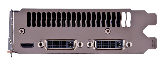
Meanwhile looking at the IO bracket for the 580, we find the same configuration as we saw on the 480. Below a full-sized vent are 2 DVI ports and a mini-HDMI port. NVIDIA slightly revised their display controller for GF110/GTX580; the good news is that HDMI 1.4a is supported, the bad news is that full audio bitstreaming is not supported so it’s the same as it was on the GTX 480: 8 channel LPCM and lossy audio formats like DD+ and DTS. This actually caught us off-guard since we were expecting the full GF104 treatment here, but it just goes to show that this is a GF100-derrivative after all. Unfortunately this also extends to the number of displays supported – NVIDIA still only supports 2 displays on one card, so you need to run in SLI if you intend to take advantage of 3DVision/NVIDIA surround across 3 monitors.
Finally, it’s with some sense of irony that we find ourselves yelling more at AMD than NVIDIA for naming shenanigans this time around, considering it was NVIDIA that brought us the 8800GT/9800GT and GeForce 200/300 product naming snafus. While NVIDIA has made some changes compared to the GTX 480, it’s a very short list; shorter than even AMD’s list for the 6800 series. At the same time, at least the GTX 580 is faster than the GTX 480 versus AMD’s 6800/5800 series. Quite frankly the GTX 580 should be the GTX 485 – the few architectural changes we’ve seen do make a difference, but then NVIDIA did a whole die shrink on the GTX 280 and only got a GTX 285 out of it. Both companies seem committed to coming out with a new family of video cards this year regardless of where the GPU powering them has actually changed. Ultimately the GTX 580 is the second flimsiest excuse for a new series number, next only to simply rebranding an existing GPU.


160 Comments
View All Comments
wtfbbqlol - Thursday, November 11, 2010 - link
Most likely an anomaly. Just compare the GTX480 to the GTX470 minimum framerate. There's no way the GTX480 is twice as fast as the GTX470.Oxford Guy - Friday, November 12, 2010 - link
It does not look like an anomaly since at least one of the few minimum frame rate tests posted by Anandtech also showed the 480 beating the 580.We need to see Unigine Heaven minimum frame rates, at the bare minimum, from Anandtech, too.
Oxford Guy - Saturday, November 13, 2010 - link
To put it more clearly... Anandtech only posted minimum frame rates for one test: Crysis.In those, we see the 480 SLI beating the 580 SLI at 1920x1200. Why is that?
It seems to fit with the pattern of the 480 being stronger in minimum frame rates in some situations -- especially Unigine -- provided that the resolution is below 2K.
I do hope someone will clear up this issue.
wtfbbqlol - Wednesday, November 10, 2010 - link
It's really disturbing how the throttling happens without any real indication. I was really excited reading about all the improvements nVidia made to the GTX580 then I read this annoying "feature".When any piece of hardware in my PC throttles, I want to know about it. Otherwise it just adds another variable when troubleshooting performance problem.
Is it a valid test to rename, say, crysis.exe to furmark.exe and see if throttling kicks in mid-game?
wtfbbqlol - Wednesday, November 10, 2010 - link
Well it looks like there is *some* official information about the current implementation of the throttling.http://nvidia.custhelp.com/cgi-bin/nvidia.cfg/php/...
Copy and paste of the message:
"NVIDIA has implemented a new power monitoring feature on GeForce GTX 580 graphics cards. Similar to our thermal protection mechanisms that protect the GPU and system from overheating, the new power monitoring feature helps protect the graphics card and system from issues caused by excessive power draw.
The feature works as follows:
• Dedicated hardware circuitry on the GTX 580 graphics card performs real-time monitoring of current and voltage on each 12V rail (6-pin, 8-pin, and PCI-Express).
• The graphics driver monitors the power levels and will dynamically adjust performance in certain stress applications such as Furmark 1.8 and OCCT if power levels exceed the card’s spec.
• Power monitoring adjusts performance only if power specs are exceeded AND if the application is one of the stress apps we have defined in our driver to monitor such as Furmark 1.8 and OCCT.
- Real world games will not throttle due to power monitoring.
- When power monitoring adjusts performance, clocks inside the chip are reduced by 50%.
Note that future drivers may update the power monitoring implementation, including the list of applications affected."
Sihastru - Wednesday, November 10, 2010 - link
I never heard anyone from the AMD camp complaining about that "feature" with their cards and all current AMD cards have it. And what would be the purpose of renaming your Crysis exe? Do you have problems with the "Crysis" name? You think the game should be called "Furmark"?So this is a non issue.
flyck - Wednesday, November 10, 2010 - link
the use of renaming is that nvidia uses name tags to identify wether it should throttle or not.... suppose person x creates a program and you use an older driver that does not include this name tag, you can break things.....Gonemad - Wednesday, November 10, 2010 - link
Big fat YES. Please do rename the executable from crysis.exe to furmark.exe, and tell us.Get furmark and go all the way around, rename it to Crysis.exe, but be sure to have a fire extinguisher in the premises. Caveat Emptor.
Perhaps just renaming in not enough, some checksumming is involved. It is pretty easy to change checksum without altering the running code, though. When compiling source code, you can insert comments in the code. When compiling, the comments are not dropped, they are compiled together with the running code. Change the comment, change the checksum. But furmark alone can do that.
Open the furmark on a hex editor and change some bytes, but try to do that in a long sequence of zeros at the end of the file. Usually compilers finish executables in round kilobytes, filling with zeros. It shouldn't harm the running code, but it changes the checksum, without changing byte size.
If it works, rename it Program X.
Ooops.
iwodo - Wednesday, November 10, 2010 - link
The good thing about GPU is that it scales VERY well ( if not linearly ) with transistors. 1 Node Die Shrink, Double the transistor account, double the performance.Combined there are not bottleneck with Memory, which GDDR5 still have lots of headroom, we are very limited by process and not the design.
techcurious - Wednesday, November 10, 2010 - link
I didnt read through ALL the comments, so maybe this was already suggested. But, can't the idle sound level be reduced simply by lowering the fan speed and compromising idle temperatures a bit? I bet you could sink below 40db if you are willing to put up with an acceptable 45 C temp instead of 37 C temp. 45 C is still an acceptable idle temp.