Intel's Sandy Bridge Architecture Exposed
by Anand Lal Shimpi on September 14, 2010 4:10 AM EST- Posted in
- CPUs
- Intel
- Sandy Bridge
Sandy Bridge Graphics
The largest performance improvement on Sandy Bridge vs. current Westmere architectures actually has nothing to do with the CPU, it’s all graphics. While the CPU cores show a 10 - 30% improvement in performance, Sandy Bridge graphics performance is easily double what Intel delivered with Clarkdale/Arrandale at the beginning of the year.
While the ‘dales improved performance by moving graphics to a 45nm process, increasing shader hardware and clock speed, SNB graphics improves through a significant increase in IPC.
The Sandy Bridge GPU is on-die built out of the same 32nm transistors as the CPU cores. The GPU is on its own power island and clock domain. The GPU can be powered down or clocked up independently of the CPU. Graphics turbo is available on both desktop and mobile parts, and you get more bins with graphics turbo on Sandy Bridge than you did with Arrandale.
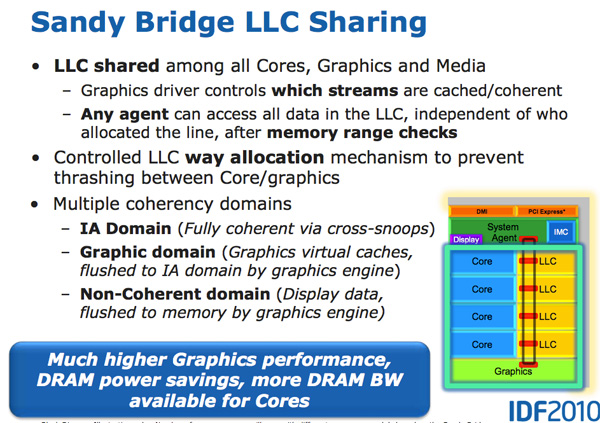
The GPU is treated like an equal citizen in the Sandy Bridge world, it gets equal access to the L3 cache. The graphics driver controls what gets into the L3 cache and you can even limit how much cache the GPU is able to use. Storing graphics data in the cache is particularly important as it saves trips to main memory which are costly from both a performance and power standpoint. Redesigning a GPU to make use of a cache isn’t a simple task. It usually requires the sort of complete re-design that NVIDIA did with GF100 for example.
SNB graphics is the anti-Larrabee. While Larrabee focused on extensive use of fully programmable hardware (with the exception of the texture hardware), SNB graphics (internally referred to as Gen 6 graphics) makes extensive use of fixed function hardware. The design mentality was anything that could be described by a fixed function should be implemented in fixed function hardware. The benefit is performance/power/die area efficiency, at the expense of flexibility. Keeping much of the GPU fixed function is in-line with Intel’s CPU centric view of the world. By contrast, taking the GPU as programmable as possible makes more sense for a GPU focused company like NVIDIA.
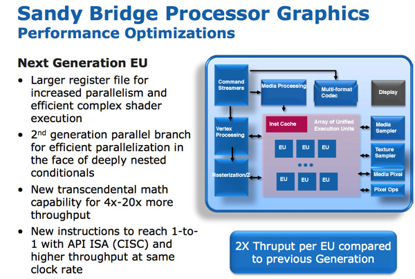
The programmable shader hardware is composed of shaders/cores/execution units that Intel calls EUs. Each EU can dual issue picking instructions from multiple threads. The internal ISA maps one-to-one with most DirectX 10 API instructions resulting in a very CISC-like architecture. Moving to one-to-one API to instruction mapping increases IPC by effectively increasing the width of the EUs.
There are other improvements within the EU. Transcendental math is handled by hardware in the EU and its performance has been sped up considerably. Intel told us that sine and cosine operations are several orders of magnitude faster now than they were in current HD Graphics.
In previous Intel graphics architectures the register file was repartitioned on the fly. If a thread needed fewer registers, the remaining registers could be allocated to another thread. While this was a great approach for saving die area, it proved to be a limiter for performance. In many cases threads couldn’t be worked on as there were no registers available for use. Prior to Intel HD Graphics each thread had an average of 64 registers, the ‘dales brought that average up to 80 per thread. In SNB, the GPU has a fixed amount of registers per thread: 120. The register count limiting thread count scenarios have been alleviated.
All of these enhancements result in 2x the instruction throughput per EU compared to Intel’s HD Graphics today.

Sandy Bridge vs. NVIDIA GeForce 310M Playing Starcraft 2
At launch there will be two versions of Sandy Bridge graphics: one with 6 EUs and one with 12 EUs. All mobile parts (at launch) will use 12 EUs, while desktop SKUs may either use 6 or 12 depending on the model. From what I’ve heard, the higher end SKUs may have 12 while the lower end models will have 6 but I haven’t seen it on a roadmap yet so I can’t confirm. With a 2x improvement in throughput per EU, you should see greater than Intel HD Graphics performance even with the 6 EU parts (thanks to higher clock speeds and the GPU sharing the L3 cache).


62 Comments
View All Comments
JoJoman88 - Wednesday, September 15, 2010 - link
To me the problem is that instead of me overclocking without reguard to TDP, now Intel will do the overclocking for me, but it will be within the TDP that Intel thinks is best. Will this not just kill the after-market cooler makers with an almost locked TDP,and to some degree high end memory maker with a locked BCLK.This will change how overclocking is done from now on unless AMD keeps things as they are and forces Intel from going down this road.
gvaley - Wednesday, September 15, 2010 - link
It's true that the CPU will turboboost within the CPU's TDP, but exactly how much it will turboboost (how much bins it will gain) will depend on how well the CPU is being chilled. So having a better (read: aftermarket) cooler will allow you to take the best of your CPU's turboboost.shodanshok - Wednesday, September 15, 2010 - link
Hi Anand,while I expect the ring bus to provide great performances, I doubt that it don't impact die size and power consumption in respect to the Nehalem/Westmere L3 organization.
Let me explain...
From my internal test, the Nehalem/Westmere L3 cache seems accessed by a four 64 bit channels (one per core). At 3 Ghz L3 cache, it translate in a maximum of 24 GB/s per core, or 96 GB/s for 4 cores. This cache organization seems confirmed by the tests at Techreport (on a i975X, SANDRA's L3 cumulative bandwidth is at about 60 GB/s: http://www.techreport.com/articles.x/18581/5) and Xbitlabs (EVEREST single-core L3 bandwidth of about 20 GB/s: http://www.xbitlabs.com/articles/cpu/display/intel...
So, on Nehalem/Westmere I do not expect 4 x 256 wires, but only 4 x 64 wires (more or less).
Now, lets examine SB...
We have 4 x 256 bit bus (4 indipendent rings) that runs around the L3 cache, for a total of 1024 wires. So, we have a lot of wires, that needs to be powered. These wires, in turn, need additional die space, and to me seems the main reason why most models will have "only" a 6 MB L3.
What do you think about? It is possible to ask Intel something about the Nehalem L3 cache organization and/or about the decision to equip most SB models with 6 MB of L3 cache?
Thanks.
Casper42 - Wednesday, September 15, 2010 - link
Knowing what you do about Nehalem EX and SNB on socket H2, any speculation on what we can expect from the Socket B2/R chips when they finally arrive sometime next year?I am mainly thinking of Northbridge/QPI and PCIe Lanes as compared to DMI used on the Mainstream parts discussed in this article.
I waited and waited for Westmere Core i7 to become "cheap" and thought the 970 was going to be my chip of choice @ $550. When they released it at $900 (you could already find 980Xs for less) it pretty much killed my plans to upgrade.
So now I am basically debating on do I build a high end H2 or wait for the enthusiast version to arrive instead?
My understanding from seeing the server roadmap is there will be Socket B2 and Socket R with the differences between them mainly consisting of memory channels and # of PCIe Lanes. I have also read that both will support PCIe 3.0 whereas H2 will continue to use 2.0.
Add all these changes up and I am also hopeful we will see USB3 on the Enthusiast platform as well since it will have an additional 3-6 months to mature.
So any ideas/insight you have here would be awesome.
linkages - Thursday, September 16, 2010 - link
With the price of LCDs dropping, I am noticing that more and more consumers have more than one display for their mainstream machines. Has Intel said anything about how many displays the onboard graphics will be able to push? Have they said anything about what tech they are going to use ie. display port, HDMI, DVI-D, something else?I can see myself getting a new SB machine sometime in Q1 2011 but I run at least 2 monitors at all times ( need the real estate for the type of work that I do ). I don't play many games but having the video decode/encode is important to me since I do tend to do some videoconferencing now a days.
The last thing I would like to know is if Intel is going to do the right thing with the drivers for their graphics. Will we humble linux users finally have a graphics driver that does not suck. Will Intel finally open source the driver so that the community can keep it updated and optimize it for X?
chukked - Thursday, September 16, 2010 - link
Hi Anand,thanks for the review, you addressed everything but left virtualization :(
which processors support vt-x and vt-d ?
iwodo - Friday, September 17, 2010 - link
x264, the best h.264 encoder there is, produce better quality video and similar speed when using "ultrafast" setting. And with 2 / 4 Core we could even transcode 2 - 4 video at the same time.The hardware encoder inside SandyBridge is not that speedy. While i could scarifies quality for speed. But Power VR's VRE Core manage 1000fps +, @ 400fps the encoder is like a waste of die space.
Intel could have further tuned the x264 for Sandy Bridge for speed and just release it with their drivers. If the hardware encoder aren't giving many times the increase in speed, then what is the point? They may as well have added extra 6 EU for GPU inside.
A Link to someone's blog posting some figures.
http://lee.hdgreetings.com/2010/09/intel-cpu-vs-nv...
Wolfpup - Wednesday, September 29, 2010 - link
Pretty disappointing. I'm sure AMD's glad though!10-30% improvement-obviously that's great, but not as big as their previous tocks if I'm remembering right, and not much different from what "ticks" like Penryn did...I know Penryn was like a 10% boost minimum over Conroe...
I'm guessing it's because they're wasting effort and die area on a worthless GPU. I *HOPE* no one on this site, no power users are going to be using that thing. (Well, okay, for a tiny notebook or something maybe...)
JumpingJack - Wednesday, September 29, 2010 - link
I don't believe you are remembering correctly.Conroe was the first tock, and certainly, it was a major leap over the P4 line. But it's bloodline was actually derived from P6, which was carried through from Banias, Dothan, then Yohna. The improvement over Yohna was in the 10-20% IPC range.
Then came Penryn the tick, which was on average only 5%, http://www.anandtech.com/show/2306/3
Then came the tock, which was Nehalem. In single threaded performance, it was roughly another 5-10% over Penryn, but in multithreaded -- again, clock for clock, it had leaps of performance, around 20-40% again. http://www.anandtech.com/show/2658/20
The tick of Nehalem was Westmere, now Westmere did not launch a quad core part so it is hard to find a clock for clock, but in single threaded performance -- roughly the same as Nehalem, factoring out any turbo advantages...
Now SB, a tick, with another 10-30% across the board both single and multithreaded, depending on workload.
Of course, the GPU is not so worthless, it is indeed challenging low end GPUs -- no doubt Llano will offer up strong GPU performance, but for the majority of the market SB is perfectly fine.
Indeed, AMD is not too happy here, at least I would suspect. On the CPU side, Intel will crush anything AMD has in the same market segement where SB resides... GPU, surely AMD will crush SB. On the CPU front, AMD is already 20-40% behind Nehalem clock for clock, core for core, SB just extends that another 10-30%.
gundersausage - Tuesday, October 26, 2010 - link
i7-950 vs i7-2500K... So which will be faster and a better gaming chip? anyone?