Intel's Sandy Bridge Architecture Exposed
by Anand Lal Shimpi on September 14, 2010 4:10 AM EST- Posted in
- CPUs
- Intel
- Sandy Bridge
Sandy Bridge Graphics
The largest performance improvement on Sandy Bridge vs. current Westmere architectures actually has nothing to do with the CPU, it’s all graphics. While the CPU cores show a 10 - 30% improvement in performance, Sandy Bridge graphics performance is easily double what Intel delivered with Clarkdale/Arrandale at the beginning of the year.
While the ‘dales improved performance by moving graphics to a 45nm process, increasing shader hardware and clock speed, SNB graphics improves through a significant increase in IPC.
The Sandy Bridge GPU is on-die built out of the same 32nm transistors as the CPU cores. The GPU is on its own power island and clock domain. The GPU can be powered down or clocked up independently of the CPU. Graphics turbo is available on both desktop and mobile parts, and you get more bins with graphics turbo on Sandy Bridge than you did with Arrandale.
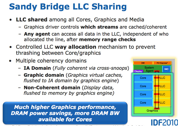
The GPU is treated like an equal citizen in the Sandy Bridge world, it gets equal access to the L3 cache. The graphics driver controls what gets into the L3 cache and you can even limit how much cache the GPU is able to use. Storing graphics data in the cache is particularly important as it saves trips to main memory which are costly from both a performance and power standpoint. Redesigning a GPU to make use of a cache isn’t a simple task. It usually requires the sort of complete re-design that NVIDIA did with GF100 for example.
SNB graphics is the anti-Larrabee. While Larrabee focused on extensive use of fully programmable hardware (with the exception of the texture hardware), SNB graphics (internally referred to as Gen 6 graphics) makes extensive use of fixed function hardware. The design mentality was anything that could be described by a fixed function should be implemented in fixed function hardware. The benefit is performance/power/die area efficiency, at the expense of flexibility. Keeping much of the GPU fixed function is in-line with Intel’s CPU centric view of the world. By contrast, taking the GPU as programmable as possible makes more sense for a GPU focused company like NVIDIA.
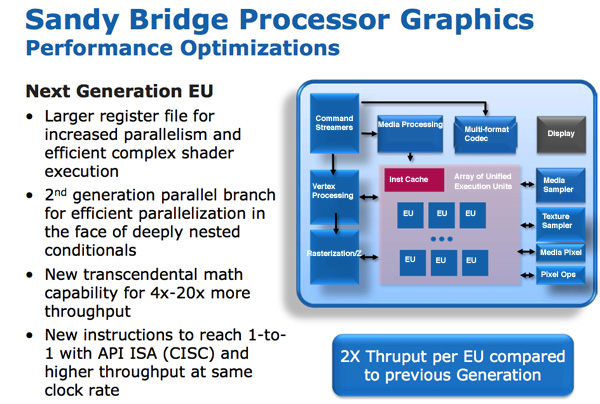
The programmable shader hardware is composed of shaders/cores/execution units that Intel calls EUs. Each EU can dual issue picking instructions from multiple threads. The internal ISA maps one-to-one with most DirectX 10 API instructions resulting in a very CISC-like architecture. Moving to one-to-one API to instruction mapping increases IPC by effectively increasing the width of the EUs.
There are other improvements within the EU. Transcendental math is handled by hardware in the EU and its performance has been sped up considerably. Intel told us that sine and cosine operations are several orders of magnitude faster now than they were in current HD Graphics.
In previous Intel graphics architectures the register file was repartitioned on the fly. If a thread needed fewer registers, the remaining registers could be allocated to another thread. While this was a great approach for saving die area, it proved to be a limiter for performance. In many cases threads couldn’t be worked on as there were no registers available for use. Prior to Intel HD Graphics each thread had an average of 64 registers, the ‘dales brought that average up to 80 per thread. In SNB, the GPU has a fixed amount of registers per thread: 120. The register count limiting thread count scenarios have been alleviated.
All of these enhancements result in 2x the instruction throughput per EU compared to Intel’s HD Graphics today.

Sandy Bridge vs. NVIDIA GeForce 310M Playing Starcraft 2
At launch there will be two versions of Sandy Bridge graphics: one with 6 EUs and one with 12 EUs. All mobile parts (at launch) will use 12 EUs, while desktop SKUs may either use 6 or 12 depending on the model. From what I’ve heard, the higher end SKUs may have 12 while the lower end models will have 6 but I haven’t seen it on a roadmap yet so I can’t confirm. With a 2x improvement in throughput per EU, you should see greater than Intel HD Graphics performance even with the 6 EU parts (thanks to higher clock speeds and the GPU sharing the L3 cache).


62 Comments
View All Comments
yuhong - Tuesday, September 14, 2010 - link
There is no VEX.256 for 256-bit integer ops, but there is a VEX.128 prefix that zeros the upper part of YMM registers to reduce the delays..NaN42 - Tuesday, September 14, 2010 - link
Well, I found a summary of the prefixes. Interestingly there are some exception, like I guessed, e.g. a VEX.128 prefix does not exist for conversion of packed floating points<->packed integers and for CRC32c + POPCNT.CSMR - Tuesday, September 14, 2010 - link
Anand:The best info available on an exciting platform, good job.
I wonder if for the next article you could test DirectX / OpenGL compatibility? Intel advertises compliance for a lot of its products, but in reality the support is partial, and some applications that use DirectX / OpenGL entirely correctly are not supported by Intel graphics, including the current HD graphics.
I've found this with fastpictureviewer (DirectX, I think 9) and Photoshop CS5 (OpenGL 2)
This is quite shocking. Given that Intel is doing this currently, it would be great if reviewers could prod it into action, but unfortunately they tend to place speed first, correctness second or nowhere.
marass31 - Thursday, September 16, 2010 - link
Hi CSMR,Could you please write more details about problems with DX and OGL on Intel HD graphics( including gfx driver version, system config ...). You mentioned about two applications: Fastpictureviewer and PSCS5, so could you please write some steps to reproduce to each of them - THX a lot.
ssj4Gogeta - Tuesday, September 14, 2010 - link
What's the point of extreme editions if we're going to have affordable K SKUs?Or will socket 2011 not have any K SKUs? I'm guessing they'll leave the BCLCK unlocked on the 2011, and only have normal and extreme processors (no K processors). Or maybe extreme editions will just have more cores like 980X?
DanNeely - Tuesday, September 14, 2010 - link
The extreme editions have always been for people who buy retail or who're playing with LN2 and need the most insanely binned part available. They've never been a mainstream OCer part.MonkeyPaw - Tuesday, September 14, 2010 - link
I have a bad feeling about the "k" chips and the future of overclocking. Sure, intel gave us turbo mode, but that almost seems like appeasement before the last shoe drops. First, limited turbo with good overclockng, then better turbo and less overclocking, and now it's sounding like slightly better turbo and even less overclocking. It looks like we are moving to intel-controlled overclocking. There's virtually no value left for the enthusiast--a user that is already just a small part of the market. Intel just decided what the enthusiast needs, but I don't think they get what those users actually want.I just don't buy that these limits are to prevent fraud. Mom and Pop stores are virtually all gone now, and I'd hate to think what Intel would do to a Dell or HP if they got caught overclocking desktops.
I guess this leaves another door open for AMD. Sad, cause SnB looks like a great design.
This Guy - Wednesday, September 15, 2010 - link
Hopefully Intel will allow the 'energy budget' to be increased when an extreme edition processer detects less thermal resistance (i.e. a bloody big heat sink). This would allow an EE CPU to either run with a higher multiplier or run at it's turbo frequency longer. (I'ld like this feature on all CPU's)This would make EE CPU's interesting if K CPU's catch up in terms of cores.
Shadowmaster625 - Tuesday, September 14, 2010 - link
What are the prospects for using Intel's transcoder to convert DVDs to 700MB avi files? Either DivX, Xvid, or H.264? Or anything else better than MPEG-2?Dfere - Tuesday, September 14, 2010 - link
Since this seems to be, overall, a refinement, and not so much an improvement with new capabilities, and Anand's comments about the scalability of GPU related enhancements, that Intel is taking a two step approach towards CPU releases, in addition to its fab strategies? E.G, we see a new CPU, then it gets shrunk, then it gets improved (like this), then it gets bells and whistles (like a GPU etc), then we start over again with a really new architecture.....