Everything You Always Wanted to Know About SDRAM (Memory): But Were Afraid to Ask
by Rajinder Gill on August 15, 2010 10:59 PM ESTWhat do you mean you've never heard of Adaptive Page Management (APM) Technology? Well, that must be because Intel Marketing doesn't seem to feel the need to bring it up.
Simply put, Intel's APM determines, based on the potential implications of pending memory transactions, whether closing open pages, or allowing them to remain open longer may be beneficial to overall memory performance. In response, the memory controller may (or may not) elect to issue commands to close pages, depending on the programmed operation.
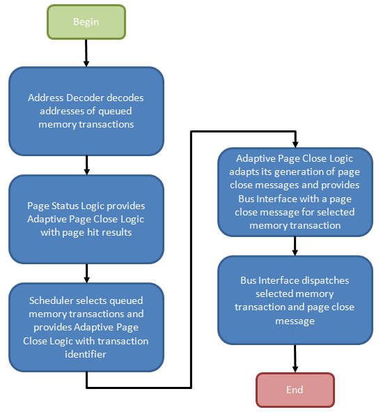
Figure 10 provides the general flow of events required to manage such a process. In our explanation we intend to introduce you to all known register settings needed to adjust the functional control policy, but first we need to detail the necessary actions, and purpose, of the design elements that make up such a mechanism. A better understanding of the underlying logic will pay dividends as you attempt to dial in measurable performance improvements through experimentation.
Per Figure 11, the Transaction Queue stores memory transactions generated by the processor. Unlike a typical First-In-First-Out (FIFO) queue with a tail, into which memory transaction may be pushed, and a head, from which memory transactions may be popped, this transaction queue is a plurality of storage elements allowing single memory transactions to be removed from the list and dispatched toward the memory in a different ordering than when originally added to the queue.
Command re-ordering can improve perceived memory performance by grouping together reads/writes to a common physical page in memory, saving the time that would otherwise be needed to later re-open the same page, should a concurrent access to the same bank force it to close early. After all, the minimum delay between sequential accesses to the same open page is equal to the CAS Latency (CL or tCAS) of the device. Accessing a bank (opening a page) increases the latency of the post-interleaved operation by the Row-Column (or Command) Delay (tRCD), approximately doubling the effective data access time.
One should also appreciate that there are varying degrees of freedom when shuffling transactions in time. Like in the case of a read and write to the same memory location: the memory controller would be disallowed from moving the dependent read either ahead of or behind the associated write as the ordering must be implicitly maintained or coherency will be lost.
The Address Decoder partially decodes the memory transactions stored in the Transaction Queue as needed to determine the bank and page selected by each queued request. From there, the Bank Select messages control the multiplexers used to input the contents of a Bank Register to a comparator used to check if the selected page was also the most recently opened page for that bank (as such, each Bank Register is large enough to store n bits where each bank comprises 2n pages). A match results in the creation of a Page-Hit Result message.
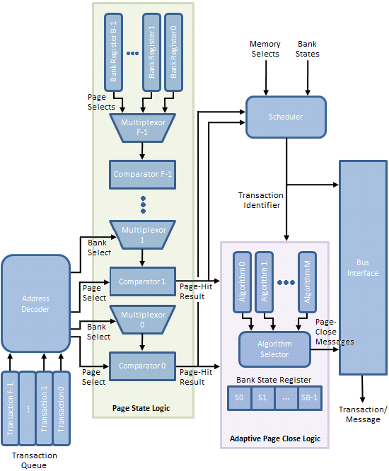
Triggered by the Page State Logic, the Scheduler fetches pre-identified queued memory transactions for re-ordering based on the Memory Selects (both bank and page) and the associated Page-Hit Results. An array of Bank State Registers track actions performed upon each bank by storing a state-word indicating, among other things, whether the Adaptive Page Close Logic decided to close the bank in response to a previous memory transaction to the same bank.
Finally, based on the policy instantiated by the Algorithm Selector, a Page-Close Message either is or is not generated based on the same Page-Hit Results, Bank State Registers, and Bank/Page Selects in an effort to increase the number of subsequent page-hit accesses and/or decrease the number of page-miss accesses.
An immediate and tangible gain is achieved for every successfully re-ordered transaction as a page-hit access is more efficient than a page-empty, or at worst, a page-miss. This is always the case with Core i7 and is one of this architecture's well known shinning points. Switch off Adaptive Page Management (disable Adaptive Page Closing in BIOS) and this is where the process ends. The page may stay open for some finite time or it may be closed right away; we're not sure as there's really no way to know without some inside help.
The Adaptive Page Close Logic must now decide whether to collect all winnings, and close the page, or let it ride, and leave it open just a while longer. While another page-hit access may yield further gains, "guessing" wrong will cause a costly page-miss access in place what would have been just a page-empty access. If only there were some way the system could measure the effectiveness of previous close decisions and then adjust policy to fit...
Surprise! The Page Manager - made up of the Page State Logic, Adaptive Page Close Logic, and Scheduler - does exactly this. How this effectiveness is measured, and how the result of that evaluation is used to adapt the decision-making process is our next topic of discussion.


46 Comments
View All Comments
bowhe - Tuesday, October 26, 2010 - link
Thanks for these great articles!What I didn't understand yet:
You state "Installing more than one DIMM per channel does not double the Memory Bus bandwidth, as modules co-located in the same channel must compete for access to a shared 64-bit sub-bus; however, adding more modules does have the added benefit of doubling the number of pages that may be open concurrently (twice the ranks for twice the fun!)". This sounds very positive, but:
Some system manufacturers state that with 3 dimms the memory frequency can be for example 1333MHz, but with 6 dimms it needs to drop to 800MHz. Why does the frequency need to drop when using 6 versus 3 dimms? Does this apply to high end boards like the Gigabyte-X58A-UD9?
Some manufacturer states in a small side note of a 24GB kit (6x4GB) that the stated frequency/timing is only guaranteed when using 3 dimm slots. This leads me to think that any 3 dimms of the set can do the stated timing, but when all are used something inherent in the design or interaction of the i7 processor, motherboard and dimm prevents the use of stated frequency/timings? What is it?
Can one overcome these limitations by adjusting voltages in a high end board like the Gigabyte-X58A-UD9? (without use of extreme cooling <32F/0C)
Thanks a lot!
kakfjak - Thursday, May 5, 2011 - link
www.stylishdudes.com
All kinds of shoes + tide bag
Free transport
cochleoid - Tuesday, March 12, 2013 - link
"When associated in groups of two (DDR), four (DDR2) or eight (DDR3), these banks form the next higher logical unit, known as a rank. "This mislead me. DDR2 may have coincidentally introduced 3 bit banks - allowing for 8 bank chips - but a typical old SDRAM (no DDR) chip had 4 banks.
"We can now see why the DDR3 core has a 8n-prefetch (where n refers to the number of banks per rank) as every read access to the memory requires a minimum of 64 bits (8 bytes) of data to be transferred. This is because each bank, of which there are eight for DDR3, fetches no less than 8 bits (1 byte) of data per read request - the equivalent of one column's worth of data. Whether or not the system actually makes use of all 8 bytes of transferred data is irrelevant. Any delivered data not actually requested can be safely disregarded as it's just a copy of what is still retained in memory."
This threw me off even more. What's happening is that the data at 8 consecutive (or otherwise close, depending on the burst mode) column addresses is being bursted on each read. "n" refers to the width of the memory chip, or the size of the "word" at a particular column address. "n" does not have any relation to the number of banks in a rank.
8 8bit-wide DDR3 chips would make a total module width of 64 bits or 8 bytes at each column address. 8 column addresses would be 64 bytes (not 8 bytes, as the article seems to suggest), which actually corresponds to the cacheline size on most PCs.
SDRAM could burst in sizes of 1,2,4,8
DDR could burst in sizes of only 2,4,8
DDR2 could burst in sizes of only 4,8
DDR3 can burst only in 8.
(All of these could burst in 8, filling the 64 byte cachline in one read operation. The difference with the generations of DDR has been a larger minimum wait in interface clock cycles as the interface got faster and the row accesses remained sluggish.)
The internal clock of SDRAM has been limited by the speed of row accesses. What the 2n,4n,8n prefetches are doing is transferring more of this data available in an open row out at higher interface speeds with the rest of the system. It has nothing to do with the banks.
SDRAM chips were segmented into independently operating banks so that parallel operations on interleaved banks could be synchronized or pipelined. 2n, 4n, and 8n prefetch buffering can be applied without independently operating banks.
ricardo_sa - Saturday, March 26, 2016 - link
Thanks for the detailed explanation. You really saved my day. Ive read this article some time ago to help me understand how a DDR3 worked (theres few detailed explanations on google) and it turned out to be the worst mistake possible. I got the concepts wrong because of the incompetence of the publisher and lost a lot of time dealing with that 8 Bank misconception about the 64 bits.So it turns out one can only write a burst at 1 bank at a time, am i right? Otherwise you could access all the 8 banks in one single write/read....
Huendli - Friday, March 13, 2015 - link
Thanks for this interesting read with much attention to detail!"a top priority [...] should be to focus development on reducing absolute minimum latency requirements for timings such as CAS and tRCD, rather than chasing raw synthetic bandwidth figures or setting outright frequency records at the expense of unduly high random access times."
The latter's exactly what happened. DDR3-1600 modules with CL7 timings were widely available at the time this article had been written. Nowadays, you only get ridiculously-named bars with equally-ridiculously monstrous heatspreaders, but more bandwidth and worse timings than ever.
Anuradha - Tuesday, March 9, 2021 - link
Each rank consists of 8 banks, OR, each rank consists of 8 ICs and each IC consists of 8 banks??