Everything You Always Wanted to Know About SDRAM (Memory): But Were Afraid to Ask
by Rajinder Gill on August 15, 2010 10:59 PM ESTSDRAM can, in many ways, be best described as a simple state machine (Figure 2) which is either idle, active, or precharging one or more open banks. As with any machine, transition from one state to another requires a minimum wait time before the system is ready to respond to subsequent requests to do additional work. These delays have a major impact on SDRAM read and write performance, and more importantly, performance of the system as a whole.
Since SDRAM memory cells are really just miniature capacitors, the charge they contain will dissipate away naturally over time due to many factors that can influence the leakage rate, including temperature. A marked reduction in stored charge can result in either data loss or data corruption. In order to prevent this from happening SDRAM must be periodically refreshed by topping off the charge contained in each individual memory cell. The frequency with which this refresh need occur depends on the silicon technology used to manufacture the core memory die and the design of the memory cell itself.
Reading or writing to a memory cell has the same effect as refreshing the selected cell by issuing a Refresh (REF) command. Unfortunately, not all cells are read from or written to during the normal course of operation and so each cell in the array must be accessed and written back (restored) before the expiration of the refresh interval. In most cases, refresh cycles involve restoring the charge along an entire page. Over the course of the entire interval, every page is accessed and subsequently restored. At the end of the interval, the process begins again. A typical Refresh Period (tREF) is hundreds to possibly a thousand or more clocks.
All banks must be precharged and idle for a minimum of the RAS Precharge (tRP) delay before the Refresh (REF) command can be applied. An address counter, internal to the device, supplies the bank address used during the course of the refresh cycle. When the refresh cycle has completed, all banks are left in the precharged (idle) state. A delay between the REF command and the next Activate (ACT) command or subsequent REF command must be greater than or equal to the Row Refresh Cycle Time (tRFC). In other words, a minimum wait of tRFC cycles is required following a refresh to an idle bank before it can be again activated for access.
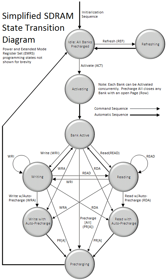
Before the SDRAM is ready to respond to read and write commands, a bank must first be opened (activated). The memory controller accomplishes this by sending the appropriate command (ACT), specifying the rank, bank, and page (row) to be accessed. The time to activate a bank is called the Row-Column (or Command) Delay and is denoted by the symbol tRCD. This variable represents the minimum time needed to latch the command at the command interface, program the control logic, and read the data from the memory array into the Sense Amplifiers in preparation for column-level access.
Following activation, the open bank contains within the array of Sense Amps a complete page of memory only 8KB in length. At this time, multiple Read (READ) and Write (WRI) commands can be issued, specifying the starting column address to be accessed. The time to read a byte of data from the open page is called the Column Address Strobe (CAS) Latency and is denoted by the symbol CL or tCAS. This variable represents the minimum time needed to latch the command at the command interface, program the control logic, gate the requested data from the Sense Amps into the Input/Output (I/O) Buffers, through a process known as pre-fetching, and place the first word of data on the Memory Bus.
Only one page per bank may be open at a time. Access to other pages in the same bank demands the open page first be closed. As long as the page remains open the memory controller can issue any combination of READ or WRI commands, sometimes switching back and forth between the two, until such time as the open page is no longer needed or a pending request to read/write data from an alternate page in the same bank requires the current page be closed so that another may be accessed. This is done by either issuing a Precharge (PR) command to close the specified bank only or a Precharge All (PRA) command to close all open banks in the rank.
Alternatively, the Precharge command can be effectively combined with the last read or write operation to the open bank by sending a Read with Auto-Precharge (RDA) or Write with Auto-Precharge (WRA) command in place of the final READ or WRI command. This allows the SDRAM control logic to automatically close the open page as soon as certain conditions have been met: (1) A minimum of RAS Activation Time (tRAS) has elapsed since the ACT command was issued, and (2) a minimum of Read to Precharge Delay (tRTP) has elapse since the most recent READ command was issued.
Precharging prepares the data lines and sense circuitry to transmit the stored charge in the Sense Amps back into the open page of individual memory cells, undoing the previous destructive read, making the DRAM core ready to sample the next page of memory to be accessed. The time to Precharge an open bank is called the Row Access Strobe (RAS) Precharge Delay and is denoted by the symbol tRP. The minimum time interval between successive ACT commands to the same bank is determined by the Row Cycle Time of the device, tRC, found by simply summing tRAS and tRP (to be defined). The minimum time interval between ACT commands to different banks is the Read-to-Read Delay (tRRD).


46 Comments
View All Comments
bowhe - Tuesday, October 26, 2010 - link
Thanks for these great articles!What I didn't understand yet:
You state "Installing more than one DIMM per channel does not double the Memory Bus bandwidth, as modules co-located in the same channel must compete for access to a shared 64-bit sub-bus; however, adding more modules does have the added benefit of doubling the number of pages that may be open concurrently (twice the ranks for twice the fun!)". This sounds very positive, but:
Some system manufacturers state that with 3 dimms the memory frequency can be for example 1333MHz, but with 6 dimms it needs to drop to 800MHz. Why does the frequency need to drop when using 6 versus 3 dimms? Does this apply to high end boards like the Gigabyte-X58A-UD9?
Some manufacturer states in a small side note of a 24GB kit (6x4GB) that the stated frequency/timing is only guaranteed when using 3 dimm slots. This leads me to think that any 3 dimms of the set can do the stated timing, but when all are used something inherent in the design or interaction of the i7 processor, motherboard and dimm prevents the use of stated frequency/timings? What is it?
Can one overcome these limitations by adjusting voltages in a high end board like the Gigabyte-X58A-UD9? (without use of extreme cooling <32F/0C)
Thanks a lot!
kakfjak - Thursday, May 5, 2011 - link
www.stylishdudes.com
All kinds of shoes + tide bag
Free transport
cochleoid - Tuesday, March 12, 2013 - link
"When associated in groups of two (DDR), four (DDR2) or eight (DDR3), these banks form the next higher logical unit, known as a rank. "This mislead me. DDR2 may have coincidentally introduced 3 bit banks - allowing for 8 bank chips - but a typical old SDRAM (no DDR) chip had 4 banks.
"We can now see why the DDR3 core has a 8n-prefetch (where n refers to the number of banks per rank) as every read access to the memory requires a minimum of 64 bits (8 bytes) of data to be transferred. This is because each bank, of which there are eight for DDR3, fetches no less than 8 bits (1 byte) of data per read request - the equivalent of one column's worth of data. Whether or not the system actually makes use of all 8 bytes of transferred data is irrelevant. Any delivered data not actually requested can be safely disregarded as it's just a copy of what is still retained in memory."
This threw me off even more. What's happening is that the data at 8 consecutive (or otherwise close, depending on the burst mode) column addresses is being bursted on each read. "n" refers to the width of the memory chip, or the size of the "word" at a particular column address. "n" does not have any relation to the number of banks in a rank.
8 8bit-wide DDR3 chips would make a total module width of 64 bits or 8 bytes at each column address. 8 column addresses would be 64 bytes (not 8 bytes, as the article seems to suggest), which actually corresponds to the cacheline size on most PCs.
SDRAM could burst in sizes of 1,2,4,8
DDR could burst in sizes of only 2,4,8
DDR2 could burst in sizes of only 4,8
DDR3 can burst only in 8.
(All of these could burst in 8, filling the 64 byte cachline in one read operation. The difference with the generations of DDR has been a larger minimum wait in interface clock cycles as the interface got faster and the row accesses remained sluggish.)
The internal clock of SDRAM has been limited by the speed of row accesses. What the 2n,4n,8n prefetches are doing is transferring more of this data available in an open row out at higher interface speeds with the rest of the system. It has nothing to do with the banks.
SDRAM chips were segmented into independently operating banks so that parallel operations on interleaved banks could be synchronized or pipelined. 2n, 4n, and 8n prefetch buffering can be applied without independently operating banks.
ricardo_sa - Saturday, March 26, 2016 - link
Thanks for the detailed explanation. You really saved my day. Ive read this article some time ago to help me understand how a DDR3 worked (theres few detailed explanations on google) and it turned out to be the worst mistake possible. I got the concepts wrong because of the incompetence of the publisher and lost a lot of time dealing with that 8 Bank misconception about the 64 bits.So it turns out one can only write a burst at 1 bank at a time, am i right? Otherwise you could access all the 8 banks in one single write/read....
Huendli - Friday, March 13, 2015 - link
Thanks for this interesting read with much attention to detail!"a top priority [...] should be to focus development on reducing absolute minimum latency requirements for timings such as CAS and tRCD, rather than chasing raw synthetic bandwidth figures or setting outright frequency records at the expense of unduly high random access times."
The latter's exactly what happened. DDR3-1600 modules with CL7 timings were widely available at the time this article had been written. Nowadays, you only get ridiculously-named bars with equally-ridiculously monstrous heatspreaders, but more bandwidth and worse timings than ever.
Anuradha - Tuesday, March 9, 2021 - link
Each rank consists of 8 banks, OR, each rank consists of 8 ICs and each IC consists of 8 banks??