Everything You Always Wanted to Know About SDRAM (Memory): But Were Afraid to Ask
by Rajinder Gill on August 15, 2010 10:59 PM ESTWhat do you mean you've never heard of Adaptive Page Management (APM) Technology? Well, that must be because Intel Marketing doesn't seem to feel the need to bring it up.
Simply put, Intel's APM determines, based on the potential implications of pending memory transactions, whether closing open pages, or allowing them to remain open longer may be beneficial to overall memory performance. In response, the memory controller may (or may not) elect to issue commands to close pages, depending on the programmed operation.
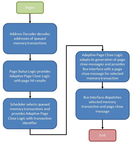
Figure 10 provides the general flow of events required to manage such a process. In our explanation we intend to introduce you to all known register settings needed to adjust the functional control policy, but first we need to detail the necessary actions, and purpose, of the design elements that make up such a mechanism. A better understanding of the underlying logic will pay dividends as you attempt to dial in measurable performance improvements through experimentation.
Per Figure 11, the Transaction Queue stores memory transactions generated by the processor. Unlike a typical First-In-First-Out (FIFO) queue with a tail, into which memory transaction may be pushed, and a head, from which memory transactions may be popped, this transaction queue is a plurality of storage elements allowing single memory transactions to be removed from the list and dispatched toward the memory in a different ordering than when originally added to the queue.
Command re-ordering can improve perceived memory performance by grouping together reads/writes to a common physical page in memory, saving the time that would otherwise be needed to later re-open the same page, should a concurrent access to the same bank force it to close early. After all, the minimum delay between sequential accesses to the same open page is equal to the CAS Latency (CL or tCAS) of the device. Accessing a bank (opening a page) increases the latency of the post-interleaved operation by the Row-Column (or Command) Delay (tRCD), approximately doubling the effective data access time.
One should also appreciate that there are varying degrees of freedom when shuffling transactions in time. Like in the case of a read and write to the same memory location: the memory controller would be disallowed from moving the dependent read either ahead of or behind the associated write as the ordering must be implicitly maintained or coherency will be lost.
The Address Decoder partially decodes the memory transactions stored in the Transaction Queue as needed to determine the bank and page selected by each queued request. From there, the Bank Select messages control the multiplexers used to input the contents of a Bank Register to a comparator used to check if the selected page was also the most recently opened page for that bank (as such, each Bank Register is large enough to store n bits where each bank comprises 2n pages). A match results in the creation of a Page-Hit Result message.
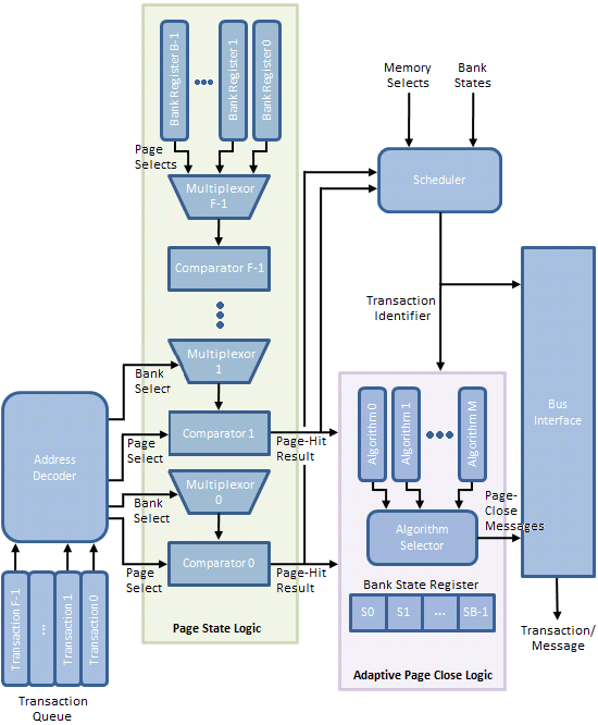
Triggered by the Page State Logic, the Scheduler fetches pre-identified queued memory transactions for re-ordering based on the Memory Selects (both bank and page) and the associated Page-Hit Results. An array of Bank State Registers track actions performed upon each bank by storing a state-word indicating, among other things, whether the Adaptive Page Close Logic decided to close the bank in response to a previous memory transaction to the same bank.
Finally, based on the policy instantiated by the Algorithm Selector, a Page-Close Message either is or is not generated based on the same Page-Hit Results, Bank State Registers, and Bank/Page Selects in an effort to increase the number of subsequent page-hit accesses and/or decrease the number of page-miss accesses.
An immediate and tangible gain is achieved for every successfully re-ordered transaction as a page-hit access is more efficient than a page-empty, or at worst, a page-miss. This is always the case with Core i7 and is one of this architecture's well known shinning points. Switch off Adaptive Page Management (disable Adaptive Page Closing in BIOS) and this is where the process ends. The page may stay open for some finite time or it may be closed right away; we're not sure as there's really no way to know without some inside help.
The Adaptive Page Close Logic must now decide whether to collect all winnings, and close the page, or let it ride, and leave it open just a while longer. While another page-hit access may yield further gains, "guessing" wrong will cause a costly page-miss access in place what would have been just a page-empty access. If only there were some way the system could measure the effectiveness of previous close decisions and then adjust policy to fit...
Surprise! The Page Manager - made up of the Page State Logic, Adaptive Page Close Logic, and Scheduler - does exactly this. How this effectiveness is measured, and how the result of that evaluation is used to adapt the decision-making process is our next topic of discussion.


46 Comments
View All Comments
ekoostik - Tuesday, August 17, 2010 - link
Great article. Going to take me a few more reads. One question - why no mention of Command Rate (and I double checked the Memory Scaling on Core i7 article, absent there too)? CR is often included in RAM specs, e.g. 9-9-9-24-2T, but never fully discussed if mentioned at all. Is it just not important anymore?Muhammed - Tuesday, August 17, 2010 - link
Ok I managed to royally confuse my self !What I know is that DDR3 operates at 1/8 the rated frequency , that means in case of DDR3 @800MHz , the internal memory operations are actually running at 100MHz , but the memory is able to fetch 8-words every clock cycle .
So 100MHz X (8 words ) = 800 Word per second as data rate , then the manufacturer misleadingly label the RAM module as a 800MHz part .
so the real benefit of DDR3 over DDR or DDR2 comes not from increased operating frequency , but from higher bandwidth .
To stress that fact , I mention DDR2 @800MHz , it operates at 200Mhz (internal clock) , however it only fetches 4-words every clock cycle , (200X4 = 800 Words).
When DDR3 operates at 200MHz (internal operations) like DDR2 , it fetches double the data , effectively managing 1600 words per second .
NOW , in your article .. you mention the base clock (I/o Bus) and you mention the double data rate , I know the I/O Bus clock is always 2 or 4 times the internal clock , so DDR3 @ 100MHz , has a 400MHz I/O bus .. but I couldn't understand the I/O bus function and it's relation in data transmission and data rate .
I am missing something here , could you enlighten me ?
Edison5do - Tuesday, August 17, 2010 - link
I Really was Affraid..!!Edison5do - Tuesday, August 17, 2010 - link
Technical Reading !!! LOve Thishasherr - Wednesday, August 18, 2010 - link
Great article. But what i dont get is how the hell motherboard knows all those timings? In SPDs there are like N timings described, isnt there really more? At least in bios settings i see more.Another thing. I buy Kingston 1800 MT/s module, with SPDs up to 1333 MTs. I overclock and make it run @ rated 1800mt/s speed. All timings are on auto. How the hell mobo/bios guess all of them :)?
ClagMaster - Wednesday, August 18, 2010 - link
Afraid to Ask ?After perusing through this I find myself afraid to read.
Comprehensive article for a novice EE
just4U - Wednesday, August 18, 2010 - link
Great article and ..." ....should be to focus development on reducing absolute minimum latency requirements for timings such as CAS and tRCD, rather than chasing.."
I hope the memory makers and shakers out there read that!!
lyeoh - Saturday, August 21, 2010 - link
The mistake counter bit counts seem OK to me. In what way are they wrong?There are 9 MSB (most significant bits) in the table.
Yes there are 13 bits in the counter, but the 9 bits in the table only refer to the 9 "top bits" of those 13 bits.
For example, if I have an 8 bit counter but 4 bits in some table only refer to the 4 most significant bits, then that means that you'd only see all zeroes in those 4 bits when the counter has values from 0 to 15 (0x0 to 0xF). When the counter has values from 240 to 255 (0xF0 to 0xFF), you'd see all ones in those 4 bits.
As for the description, I don't know the details of how the stuff works, so I don't know whether it's wrong or not.
dia - Saturday, August 21, 2010 - link
Read the explanation here:http://download.intel.com/design/processor/datasht...
Page 79.
To quote:
"MISTAKECOUNTER.
This field is the upper 8 MSBs of a 12-bit counter. This counter adapts the
interval between assertions of the page close flag. For a less aggressive page
close, the length of the count interval is increased and vice versa for a more
aggressive page close policy."
Now look at the left hand column, it shows 8:0. That's 9 bits! It's a 13 bit counter.
If it were a 12 bit counter the maximum permissible selection value would be 4095 and not 8191.
datasegment - Saturday, August 21, 2010 - link
Quick fyi - 8k is not 8196, it is 8192 :)