Everything You Always Wanted to Know About SDRAM (Memory): But Were Afraid to Ask
by Rajinder Gill on August 15, 2010 10:59 PM ESTEvery read/write memory transaction can be segmented by type into one of three performance bins depending on the status of the bank/page to be accessed. These bins, in order of best to worst, are page-hit, page-empty, and page-miss. For the most part, anything we can do to increase the number of page-hit transactions or reduce the number of page-miss transactions is a good thing.
A page-hit access is defined as any read or write operation to an open page. That is, the bank containing the open page is already active and is immediately ready to service requests. Because the target page is already open, the nominal access latency for any memory transaction falling into this category is approximately tCAS (the CAS Latency of the device).
Click to enlarge
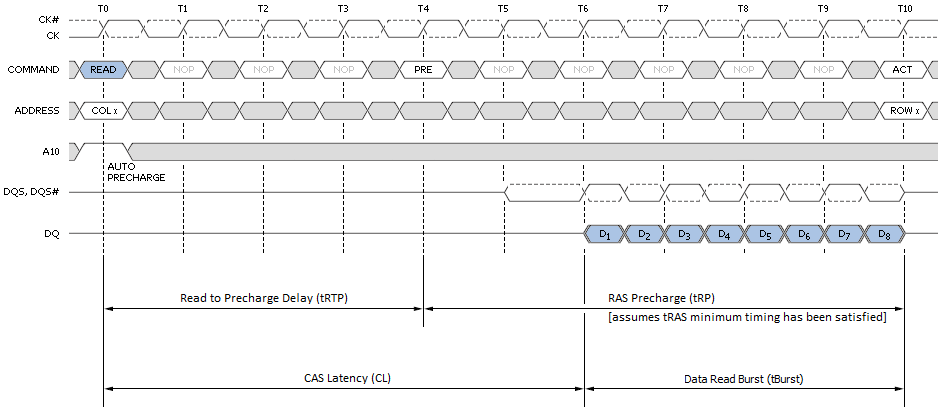
Figure 6 shows the minimum read latency associated with a best-case page-hit scenario. For a part with a CAS Latency of 6T, the memory controller waits only six short clocks before the start of data return. During a Read with Auto-Precharge, the Read command will execute as normal except the active bank will begin precharging CAS-latency (CL) clock cycles before the end of the burst. This feature allows the precharge operation to be partially or completely hidden during periods of burst read cycles, dependent on CL. When tuning our systems we always seek to set tRTP such that tRTP + tRP equals CL + tBurst for exactly this reason. Put another way, if CL and tRP are the same set 4T for DDR3 (2T for DD2).
Sequential reads to the same page make these types of transactions even more profitable as each successive access can be scheduled at a minimum of tBurst (4T) clocks from the last. The timing is captured as the CAS-to-CAS Delay (tCCD) and is commonly referred to as 'Back-to-Back CAS Delay' (B2B), as shown per Figure 7. This feature makes possible extremely high data transfer rates for total burst lengths of one page or less - in our case, 8KB.

Click to enlarge
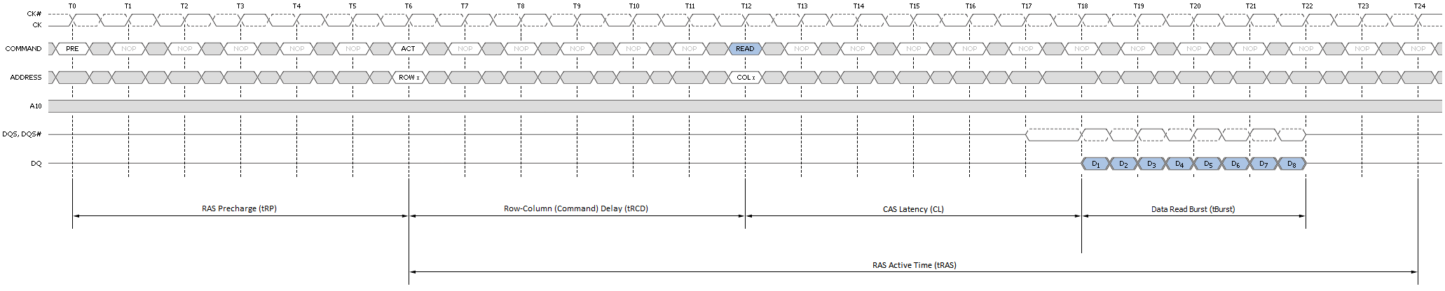
Although not ideal, a page-empty access is still preferred to a miss. In this case the bank to be accessed is Idle with no page open. Common sense tells us any attempt to read or write data to a page in this bank first requires we Activate the bank. In other words, nominal access latency now includes the time to open the page - Row-Column (or Command) Delay (tRCD). This is a doubling of the minimum access latency when compared to that of the page-hit case! Twelve cycles (tRCD + CL) now elapse before the first word is returned. Figure 8 shows this the detail.
![]()
Click to enlarge
Finally, as if the relative penalty of page-empty access wasn't bad enough, here comes page-miss. A miss occurs anytime a memory transaction must first close an open page in order to open an alternate page in the same bank. Only then can the specified data access take place. First closing an open page requires a Precharge, adding the RAS Precharge (tRP) delay to any already lengthy operation. As you can see by Figure 9, the nominal latency of an access of this type is three times that of one page-hit operation!
Click to enlarge
The relative gain/loss ratio for each access type can be quickly assessed simply through a cursory review of the most basic device timings. Imagine a memory kit rated for operation at DDR3-1600, 6-6-6-18 (CL-tRCD-tRP-tRAS): With nothing more we can estimate six cycles for a page-hit access, 12 cycles for a page-empty access, and 18 cycles for a page-miss access.
Normalized to the page-hit access latency, page-empty access is twice as long, and page-miss access is a whole three times as long. If we combine this with what we know about the inner functions of the SDRAM state machine we see page-hit and page-miss are really just subsets of the same bank state (active). Of course, page-empty access necessarily implies an idle bank. The following proof rewards us with some powerful insight.
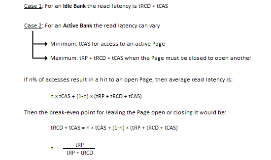
The variable n also represents the percentage of accesses to banks with open pages that must result in a page-hit access if we are to simply pace the nominal access latency that would be achieved if every read access was to an idle bank. And the only thing this depends on is the RAS Precharge delay and the Row-Column (or Command) Delay of the device in question.
You would think by working to maximize n, performance would be maximized as well. And you'd be right. Let's take what we've learned thus far and step it up a notch. We promise, after this you'll never see memory timings in the same light ever again.
Before proceeding, we've prepared a video for those of you that would like to view a few simple animations meant to help visualize each transaction type:


46 Comments
View All Comments
JarredWalton - Monday, August 16, 2010 - link
Oh, it's missing a lot more than just voltage information. :-) There are rebates on most memory kits right now, for instance. Still, I felt it was useful to highlight where the current "best deals" tend to fall.I personally wouldn't touch the ultra-expensive $150+ stuff, but up to $115 has potential at least. For a lower voltage kit, G.Skill has an ECO line rated at DDR3-1600 7-8-7-24-2N and 1.35V for $103. Worth a look at least....
JarredWalton - Monday, August 16, 2010 - link
Note: I screwed up my table above. DDR3 is two bits per clock, so the base clocks are all twice what I listed, which means latency for CAS is half what I listed. Sorry. Got things confused with GDDR5. :-) The relative latency is still the same, of course, which is the main point.JarredWalton - Monday, August 16, 2010 - link
Side note number two: And of course, CAS Latency isn't the be-all, end-all. According to benchmarks by Raja, DDR3-2000 at 6-9-6 timings often trails RAM at 7-8-7, as the tRCD difference becomes more pronounced in some cases.Rajinder Gill - Monday, August 16, 2010 - link
Sorry I should have said 7-7-8 vs 6-9-8. This happens when the number of random access requests are high (fewer back to back reads). Benchmarks like WinRar and Super Pi (synthetic) are mainly the ones that show this.-Raja
Drag0nFire - Friday, August 20, 2010 - link
I've had great experience with the ECO line. Put the 2x2 kit you mentioned in two computers so far, and it's been great. Feels like a steal to get such high speed and low voltage at such a great price.kalniel - Monday, August 16, 2010 - link
Thanks for taking the time to write the article - the cycle time-line figures are very helpful, but I'm struggling to understand it correctly.Take fig. 5. There doesn't seem to be a Read to Precharge Delay. If we follow the recommendation of CL+tBurst = tRCP + tRP then won't there be a delay of 4T after the Data Read Burst before the RAS Precharge starts, giving a Row Cycle Time of 26 rather than 24?
kjboughton - Monday, August 16, 2010 - link
tRTP may very well be 4T but the minimum RAS Active Time (tRAS) is 18T. The precharge is precluded from occuring until this period has expired making the clock at T + 18 the first opportunity to precharge the bank. Add to this the RAS Precharge (tRP) and you have the Row Cycle Time (tRC = tRAS + tRP) - the minimum time any single row MUST remain open before it can be closed (and before another page in the same bank can be accessed).Does this help?
kalniel - Monday, August 16, 2010 - link
I thought the Read to Precharge Delay was there precisely to ensure you waited the minimum RAS active time before precharging the bank. Are you saying that the tRTP doesn't apply if you've already finished tRCD+CL+tBurst within tRAS so can start precharging as soon as minimum RAS active time is achieved?In other words, tRTP doesn't have a bearing on a single burst per page, but is there to help synchronise auto-precharge reads within the same page?
My ignorance may be beyond redemption!
kjboughton - Monday, August 16, 2010 - link
Read to Precharge Delay (tRTP) is the minimum wait time from a READ (column access) to bank PRECHARGE.RAS Active Time (tRAS) is the minimum wait time from an ACTIVATE (row access) to bank PRECHARGE.
Both times must be satisfied before the bank can be precharged. Perhaps I wasn't quite clear enough on this point. I hope this clears things up.
kalniel - Monday, August 16, 2010 - link
I think I've got it now, thanks. My brain saw the relevant diagram and screamed 'Cthulu' instead.