Everything You Always Wanted to Know About SDRAM (Memory): But Were Afraid to Ask
by Rajinder Gill on August 15, 2010 10:59 PM ESTSDRAM can, in many ways, be best described as a simple state machine (Figure 2) which is either idle, active, or precharging one or more open banks. As with any machine, transition from one state to another requires a minimum wait time before the system is ready to respond to subsequent requests to do additional work. These delays have a major impact on SDRAM read and write performance, and more importantly, performance of the system as a whole.
Since SDRAM memory cells are really just miniature capacitors, the charge they contain will dissipate away naturally over time due to many factors that can influence the leakage rate, including temperature. A marked reduction in stored charge can result in either data loss or data corruption. In order to prevent this from happening SDRAM must be periodically refreshed by topping off the charge contained in each individual memory cell. The frequency with which this refresh need occur depends on the silicon technology used to manufacture the core memory die and the design of the memory cell itself.
Reading or writing to a memory cell has the same effect as refreshing the selected cell by issuing a Refresh (REF) command. Unfortunately, not all cells are read from or written to during the normal course of operation and so each cell in the array must be accessed and written back (restored) before the expiration of the refresh interval. In most cases, refresh cycles involve restoring the charge along an entire page. Over the course of the entire interval, every page is accessed and subsequently restored. At the end of the interval, the process begins again. A typical Refresh Period (tREF) is hundreds to possibly a thousand or more clocks.
All banks must be precharged and idle for a minimum of the RAS Precharge (tRP) delay before the Refresh (REF) command can be applied. An address counter, internal to the device, supplies the bank address used during the course of the refresh cycle. When the refresh cycle has completed, all banks are left in the precharged (idle) state. A delay between the REF command and the next Activate (ACT) command or subsequent REF command must be greater than or equal to the Row Refresh Cycle Time (tRFC). In other words, a minimum wait of tRFC cycles is required following a refresh to an idle bank before it can be again activated for access.
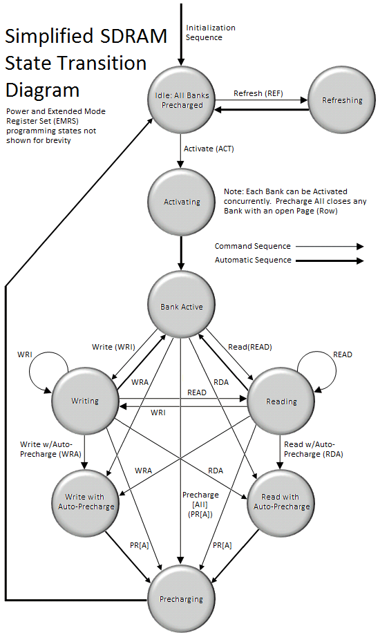
Before the SDRAM is ready to respond to read and write commands, a bank must first be opened (activated). The memory controller accomplishes this by sending the appropriate command (ACT), specifying the rank, bank, and page (row) to be accessed. The time to activate a bank is called the Row-Column (or Command) Delay and is denoted by the symbol tRCD. This variable represents the minimum time needed to latch the command at the command interface, program the control logic, and read the data from the memory array into the Sense Amplifiers in preparation for column-level access.
Following activation, the open bank contains within the array of Sense Amps a complete page of memory only 8KB in length. At this time, multiple Read (READ) and Write (WRI) commands can be issued, specifying the starting column address to be accessed. The time to read a byte of data from the open page is called the Column Address Strobe (CAS) Latency and is denoted by the symbol CL or tCAS. This variable represents the minimum time needed to latch the command at the command interface, program the control logic, gate the requested data from the Sense Amps into the Input/Output (I/O) Buffers, through a process known as pre-fetching, and place the first word of data on the Memory Bus.
Only one page per bank may be open at a time. Access to other pages in the same bank demands the open page first be closed. As long as the page remains open the memory controller can issue any combination of READ or WRI commands, sometimes switching back and forth between the two, until such time as the open page is no longer needed or a pending request to read/write data from an alternate page in the same bank requires the current page be closed so that another may be accessed. This is done by either issuing a Precharge (PR) command to close the specified bank only or a Precharge All (PRA) command to close all open banks in the rank.
Alternatively, the Precharge command can be effectively combined with the last read or write operation to the open bank by sending a Read with Auto-Precharge (RDA) or Write with Auto-Precharge (WRA) command in place of the final READ or WRI command. This allows the SDRAM control logic to automatically close the open page as soon as certain conditions have been met: (1) A minimum of RAS Activation Time (tRAS) has elapsed since the ACT command was issued, and (2) a minimum of Read to Precharge Delay (tRTP) has elapse since the most recent READ command was issued.
Precharging prepares the data lines and sense circuitry to transmit the stored charge in the Sense Amps back into the open page of individual memory cells, undoing the previous destructive read, making the DRAM core ready to sample the next page of memory to be accessed. The time to Precharge an open bank is called the Row Access Strobe (RAS) Precharge Delay and is denoted by the symbol tRP. The minimum time interval between successive ACT commands to the same bank is determined by the Row Cycle Time of the device, tRC, found by simply summing tRAS and tRP (to be defined). The minimum time interval between ACT commands to different banks is the Read-to-Read Delay (tRRD).


46 Comments
View All Comments
JarredWalton - Monday, August 16, 2010 - link
Oh, it's missing a lot more than just voltage information. :-) There are rebates on most memory kits right now, for instance. Still, I felt it was useful to highlight where the current "best deals" tend to fall.I personally wouldn't touch the ultra-expensive $150+ stuff, but up to $115 has potential at least. For a lower voltage kit, G.Skill has an ECO line rated at DDR3-1600 7-8-7-24-2N and 1.35V for $103. Worth a look at least....
JarredWalton - Monday, August 16, 2010 - link
Note: I screwed up my table above. DDR3 is two bits per clock, so the base clocks are all twice what I listed, which means latency for CAS is half what I listed. Sorry. Got things confused with GDDR5. :-) The relative latency is still the same, of course, which is the main point.JarredWalton - Monday, August 16, 2010 - link
Side note number two: And of course, CAS Latency isn't the be-all, end-all. According to benchmarks by Raja, DDR3-2000 at 6-9-6 timings often trails RAM at 7-8-7, as the tRCD difference becomes more pronounced in some cases.Rajinder Gill - Monday, August 16, 2010 - link
Sorry I should have said 7-7-8 vs 6-9-8. This happens when the number of random access requests are high (fewer back to back reads). Benchmarks like WinRar and Super Pi (synthetic) are mainly the ones that show this.-Raja
Drag0nFire - Friday, August 20, 2010 - link
I've had great experience with the ECO line. Put the 2x2 kit you mentioned in two computers so far, and it's been great. Feels like a steal to get such high speed and low voltage at such a great price.kalniel - Monday, August 16, 2010 - link
Thanks for taking the time to write the article - the cycle time-line figures are very helpful, but I'm struggling to understand it correctly.Take fig. 5. There doesn't seem to be a Read to Precharge Delay. If we follow the recommendation of CL+tBurst = tRCP + tRP then won't there be a delay of 4T after the Data Read Burst before the RAS Precharge starts, giving a Row Cycle Time of 26 rather than 24?
kjboughton - Monday, August 16, 2010 - link
tRTP may very well be 4T but the minimum RAS Active Time (tRAS) is 18T. The precharge is precluded from occuring until this period has expired making the clock at T + 18 the first opportunity to precharge the bank. Add to this the RAS Precharge (tRP) and you have the Row Cycle Time (tRC = tRAS + tRP) - the minimum time any single row MUST remain open before it can be closed (and before another page in the same bank can be accessed).Does this help?
kalniel - Monday, August 16, 2010 - link
I thought the Read to Precharge Delay was there precisely to ensure you waited the minimum RAS active time before precharging the bank. Are you saying that the tRTP doesn't apply if you've already finished tRCD+CL+tBurst within tRAS so can start precharging as soon as minimum RAS active time is achieved?In other words, tRTP doesn't have a bearing on a single burst per page, but is there to help synchronise auto-precharge reads within the same page?
My ignorance may be beyond redemption!
kjboughton - Monday, August 16, 2010 - link
Read to Precharge Delay (tRTP) is the minimum wait time from a READ (column access) to bank PRECHARGE.RAS Active Time (tRAS) is the minimum wait time from an ACTIVATE (row access) to bank PRECHARGE.
Both times must be satisfied before the bank can be precharged. Perhaps I wasn't quite clear enough on this point. I hope this clears things up.
kalniel - Monday, August 16, 2010 - link
I think I've got it now, thanks. My brain saw the relevant diagram and screamed 'Cthulu' instead.