Everything You Always Wanted to Know About SDRAM (Memory): But Were Afraid to Ask
by Rajinder Gill on August 15, 2010 10:59 PM ESTSDRAM can, in many ways, be best described as a simple state machine (Figure 2) which is either idle, active, or precharging one or more open banks. As with any machine, transition from one state to another requires a minimum wait time before the system is ready to respond to subsequent requests to do additional work. These delays have a major impact on SDRAM read and write performance, and more importantly, performance of the system as a whole.
Since SDRAM memory cells are really just miniature capacitors, the charge they contain will dissipate away naturally over time due to many factors that can influence the leakage rate, including temperature. A marked reduction in stored charge can result in either data loss or data corruption. In order to prevent this from happening SDRAM must be periodically refreshed by topping off the charge contained in each individual memory cell. The frequency with which this refresh need occur depends on the silicon technology used to manufacture the core memory die and the design of the memory cell itself.
Reading or writing to a memory cell has the same effect as refreshing the selected cell by issuing a Refresh (REF) command. Unfortunately, not all cells are read from or written to during the normal course of operation and so each cell in the array must be accessed and written back (restored) before the expiration of the refresh interval. In most cases, refresh cycles involve restoring the charge along an entire page. Over the course of the entire interval, every page is accessed and subsequently restored. At the end of the interval, the process begins again. A typical Refresh Period (tREF) is hundreds to possibly a thousand or more clocks.
All banks must be precharged and idle for a minimum of the RAS Precharge (tRP) delay before the Refresh (REF) command can be applied. An address counter, internal to the device, supplies the bank address used during the course of the refresh cycle. When the refresh cycle has completed, all banks are left in the precharged (idle) state. A delay between the REF command and the next Activate (ACT) command or subsequent REF command must be greater than or equal to the Row Refresh Cycle Time (tRFC). In other words, a minimum wait of tRFC cycles is required following a refresh to an idle bank before it can be again activated for access.
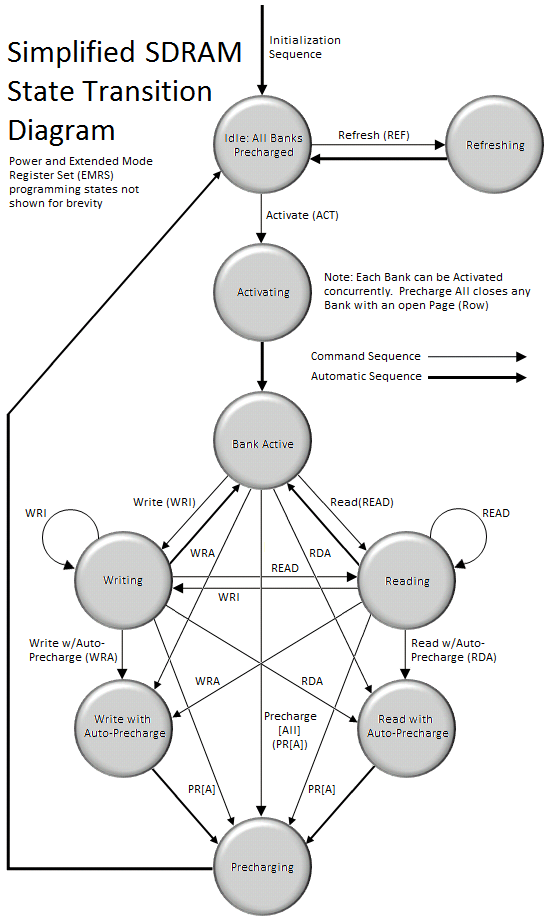
Before the SDRAM is ready to respond to read and write commands, a bank must first be opened (activated). The memory controller accomplishes this by sending the appropriate command (ACT), specifying the rank, bank, and page (row) to be accessed. The time to activate a bank is called the Row-Column (or Command) Delay and is denoted by the symbol tRCD. This variable represents the minimum time needed to latch the command at the command interface, program the control logic, and read the data from the memory array into the Sense Amplifiers in preparation for column-level access.
Following activation, the open bank contains within the array of Sense Amps a complete page of memory only 8KB in length. At this time, multiple Read (READ) and Write (WRI) commands can be issued, specifying the starting column address to be accessed. The time to read a byte of data from the open page is called the Column Address Strobe (CAS) Latency and is denoted by the symbol CL or tCAS. This variable represents the minimum time needed to latch the command at the command interface, program the control logic, gate the requested data from the Sense Amps into the Input/Output (I/O) Buffers, through a process known as pre-fetching, and place the first word of data on the Memory Bus.
Only one page per bank may be open at a time. Access to other pages in the same bank demands the open page first be closed. As long as the page remains open the memory controller can issue any combination of READ or WRI commands, sometimes switching back and forth between the two, until such time as the open page is no longer needed or a pending request to read/write data from an alternate page in the same bank requires the current page be closed so that another may be accessed. This is done by either issuing a Precharge (PR) command to close the specified bank only or a Precharge All (PRA) command to close all open banks in the rank.
Alternatively, the Precharge command can be effectively combined with the last read or write operation to the open bank by sending a Read with Auto-Precharge (RDA) or Write with Auto-Precharge (WRA) command in place of the final READ or WRI command. This allows the SDRAM control logic to automatically close the open page as soon as certain conditions have been met: (1) A minimum of RAS Activation Time (tRAS) has elapsed since the ACT command was issued, and (2) a minimum of Read to Precharge Delay (tRTP) has elapse since the most recent READ command was issued.
Precharging prepares the data lines and sense circuitry to transmit the stored charge in the Sense Amps back into the open page of individual memory cells, undoing the previous destructive read, making the DRAM core ready to sample the next page of memory to be accessed. The time to Precharge an open bank is called the Row Access Strobe (RAS) Precharge Delay and is denoted by the symbol tRP. The minimum time interval between successive ACT commands to the same bank is determined by the Row Cycle Time of the device, tRC, found by simply summing tRAS and tRP (to be defined). The minimum time interval between ACT commands to different banks is the Read-to-Read Delay (tRRD).


46 Comments
View All Comments
Dwebtron - Monday, August 16, 2010 - link
How did you know I was afraid to ask!!0ldman79 - Tuesday, May 28, 2019 - link
It's because we're all from the future.neslog - Monday, August 16, 2010 - link
Thank you for a great article on memory and you are right, I was afraid to ask.landerf - Monday, August 16, 2010 - link
I've found for the i7 platform the perfect ram setup is 1200 Mhz + cas5 or 6 timings, a 3:1 uncore ratio, and a B2B of 4. Not only does this perform well even in synthetics, it provides the "smoothest" intel experience. Something people who use amd and intel have been complaining about intel lacking. Check this chart and see how well that setup performs compared to all the conventional 2:1 setups. https://spreadsheets.google.com/ccc?key=0AsaXlcTga...Servando Silva - Monday, August 16, 2010 - link
Thanks for a great article. It will take me a while to read it carefully and fully understand it.Kris + Raju = Killer combo.
neslog - Monday, August 16, 2010 - link
On page 8 you may want to change the wording in the last paragraph " Once you've had...to cordially invite[d] (you) to do some..."
Thanks again for the article. I appreciate all the work that went into putting it together
elforeign - Monday, August 16, 2010 - link
It's a site willing to go the extra mile like this to report and educate the masses that are truly worth the time to peruse and read the posted articles. I check this site daily because there is always something interesting to read. Thank you to all the staff who do a great job here!chizow - Monday, August 16, 2010 - link
Just kidding....Or am I? :D
JarredWalton - Monday, August 16, 2010 - link
There's obviously benefits to either direction. Reducing latency is definitely a priority, but something not mentioned in the text that bears repeating is that latency is a factor of clock speed as well as the various timings. While CAS 6 will always be better than CAS 7 at the same base clock (and likewise for the other timings), if you have a faster memory speed CAS 7 could end up being better.So here's the scoop:
DDR3-1066 = 266MHz base clock, or 3.75ns per cycle.
DDR3-1333 = 333MHz base clock, or 3.00ns per cycle.
DDR3-1600 = 400MHz base clock, or 2.50ns per cycle.
DDR3-2000 = 500MHz base clock, or 2.00ns per cycle.
That gives this table in order of increasing latency, with rough pricing for 2x2GB. Based on pricing and latency, I've starred the best buys on Newegg:
CAS 6 DDR3-2000 = 12.0ns. ($180)
CAS 7 DDR3-2000 = 14.0ns. ($140)
CAS 6 DDR3-1600 = 15.0ns. ($115) ***
CAS 8 DDR3-2000 = 16.0ns. ($150)
CAS 7 DDR3-1600 = 17.5ns. ($101) ***
CAS 9 DDR3-2000 = 18.0ns. ($100) ***
CAS 6 DDR3-1333 = 18.0ns. ($100) ***
CAS 10 DDR3-2000 = 20.0ns. ($118)
CAS 8 DDR3-1600 = 20.0ns. ($85) ***
CAS 7 DDR3-1333 = 21.0ns. ($90)
CAS 9 DDR3-1600 = 22.5ns. ($92)
CAS 8 DDR3-1333 = 24.0ns. ($92)
CAS 7 DDR3-1066 = 26.3ns. ($80)
CAS 9 DDR3-1333 = 27.0ns. ($85)
CAS 8 DDR3-1066 = 30.0ns. ($93)
Notice how the total latency often comes in groups. The DDR3-1333 CL6, DDR3-1600 CL7, and DDR3-2000 CL9 are all priced around $100. If you buy any of these modules, there's a good chance (though YMMV) that you can tweak timings to run at whichever value makes you happiest. I'd probably err on the side of buying the higher speed rated modules, though, or at least grab the 1600MHz set.
Rick83 - Monday, August 16, 2010 - link
Your pricing comparison is sadly missing one important factor:Operating voltage.
I was at first surprised by the high cost of 1333/9, but I expect the voltage of that kit to be around 1.5, where most 1333/7 kits already clock in at 1.65.
The 2000/9 kit probably also runs higher V's than the identically priced 1333/6?
Lower voltages are usually preferred, as they give you a) more headroom and b) less heat at stock - with on-die controllers even less cpu heat.