Intel's 50Gbps Silicon Photonics Link: The Future of Interfaces
by Brian Klug on July 30, 2010 6:49 AM EST- Posted in
- Trade Shows
- Intel
- Photonics
- Laser
Why use light instead of copper?
High speed PCB design is already a science in and of itself. Timing requirements dictate equal path lengths for a growing number traces between components, resulting in the ever familiar squiggly designs on desktop motherboards. Higher frequencies of course also require considerations about wave propagation through the medium - just like a transmission line. At 1 GHz, for example, one wavelength is about 0.14 meters for copper traces on FR-4, one of the most common PCB materials.
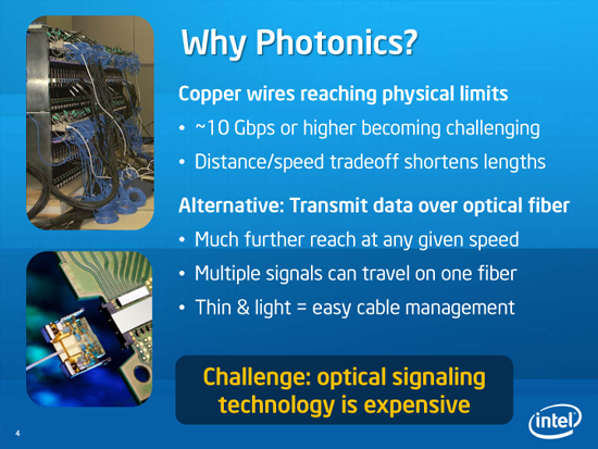
There’s also propagation delay - for wires, commonly given as 1 ns for every 6 inches of length, though different media have different wave propagation speeds due to the dielectric of the medium. I could go on about the challenges of very high frequency circuit design - which I’m not an expert in by any stretch of the mind.
The end takeaway is that traditional microelectronic designs are becoming physically constrained in size with higher and higher frequencies. You physically need to have the CPU close to the memory controller, northbridge, and other components for it to work at frequencies people expect. Move it relatively far (one wavelength) away, and the design challenges start to stretch microelectronics to its limit. Ultimately, designs sacrifice speed for distance, or vice versa.
The advantages of using optical interconnects instead of traditional copper traces are numerous. Using light instead of copper promises vastly higher bandwidth, reduced latency, resistance to electromagnetic interference, and potentially even power savings.
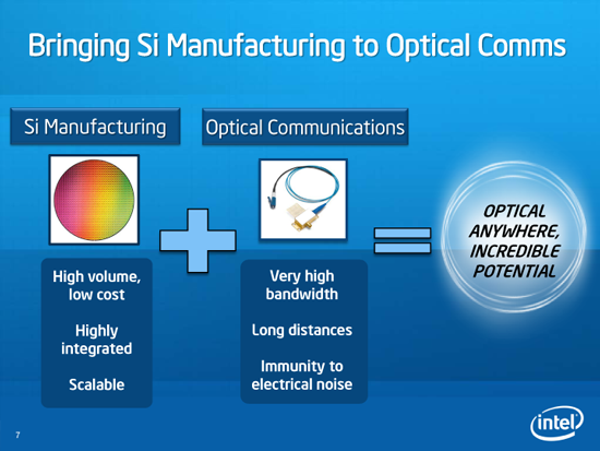
All of these reasons make using optical, silicon waveguides instead of copper traces an obvious choice. Instead of using numerous copper traces to connect the CPU to the northbridge, for example, one could envision using a single optical fiber. Or having many CPUs on one massive board connect to a chipset located even meters of path distance away. Or even have one room full of just CPUs and another room full of memory.
What Intel demonstrated on Tuesday is a working example of just that - an optical interconnect fabricated using the current traditional CMOS process, for connecting conventional electronics. Effectively an optical bus on silicon.
What’s different about Intel’s demonstration is that the lasers themselves are hybrid silicon.


42 Comments
View All Comments
ghot - Thursday, August 5, 2010 - link
"Blinded by the light...." I'm 53 years old and having been waiting for this since the 1st TI calculator hit the market in 1976. Unfortunately I probably won't live to see the 1st totally optical, consumer affordable PC.This doesn't prove 'Murphy's Law....it squares or even cubes it.
The best part, isn't even the speed (although it will be incredible) but rather the fact that PCB printed circuits can be a long as the design requires. Imagine a motherboard 5 inches wide and 3-4 foot tall. Then a PC enclosure could look more like a 4 foot tall 6x6 inch speaker enclosure for example.
Cooling needs will be greatly reduced as well. Just try to imagine the over clocking potential.
I used to drool over the 1st commercially available digital watch...the Pulsar....didn't even have LED's...it used tiny Nixie Tubes.....and now this.
When most of you are my age, you'll be complaining that your brand new Intel P4 (yes P4..maybe in YOUR lifetime, Intel will get back to simple naming schemes) is only capable of 4Thz on air. And, as every over clocker knows....increase the speeds in small increments...say .....10Ghz each time...lol
I am so jealous :)
ziaullahk - Sunday, February 18, 2018 - link
And to think about it, we just reached 100GBps according to https://compoundtek.com/news