NVIDIA’s GeForce GTX 460: The $200 King
by Ryan Smith on July 11, 2010 11:54 PM EST- Posted in
- GPUs
- GeForce GTX 400
- GeForce GTX 460
- NVIDIA
GF104: NVIDIA Goes Superscalar
When the complete GF100 GPU was presented to us back at CES 2010 in January, NVIDIA laid out a design that in turn had a very obvious roadmap to go with it. With GF100’s modular design, derivatives of the card would be as simple as fabricating GPUs with fewer GPCs and ROPs (at least until you got to the sub-$100 market). This is the route we expected NVIDIA to take with GF104, removing 1 or 2 GPCs to make a smaller chip.
What they threw us instead was a curveball we were not expecting.
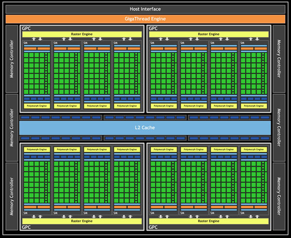
Let’s start at a high level. On GF100, there were 4 GPCs each containing a Raster Engine and 4 SMs. In turn each SM contained 32 CUDA cores, 16 load/store units, 4 special function units, 4 texture units, 2 warp schedulers with 1 dispatch unit each, 1 Polymorph unit (containing NVIDIA’s tessellator) and then the L1 cache, registers, and other glue that brought an SM together.
NVIDIA GF100 - Full Implementation, No Disabled Logic
GF104 in turn contains 2 GPCs, which are effectively the same as a GF100 GPC. Each GPC contains 4 SMs and a Raster Engine. However when we get to GF104’s SMs, we find something that has all the same parts as a GF100 SM, but in much different numbers.
NVIDIA GF104 - Full Implementation, No Disabled Logic
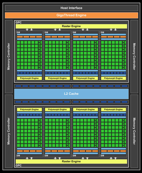
The biggest and most visible change is that NVIDIA beefed up the number of various execution units per SM. The 32 CUDA cores from GF100 are now 48 CUDA cores, while the number of SFUs went from 4 to 8 along with the texture units. As a result, per SM GF104 has more compute and more texturing power than a GF100 SM. This is how a “full” GF104 GPU has 384 CUDA cores even though it only has half the number of SMs as GF100.
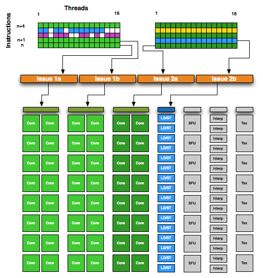
One thing we haven’t discussed up until now is how an SM is internally divided up for the purposes of executing instructions. Since the introduction of G80 in 2006, the size of a warp has stayed constant at 32 threads wide. For Fermi, a warp is executed over 2 (or more) clocks of the CUDA cores – 16 threads are processed and then the other 16 threads in that warp are processed. For full SM utilization, all threads must be running the same instruction at the same time. For these reasons a SM is internally divided up in to a number of execution units that a single dispatch unit can dispatch work to:
- 16 CUDA cores (#1)
- 16 CUDA cores (#2)
- 16 Load/Store Units
- 16 Interpolation SFUs (not on NVIDIA's diagrams)
- 4 Special Function SFUs
- 4 Texture Units
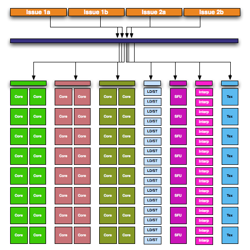
With 2 warp scheduler/dispatch unit pairs in each SM, GF100 can utilize at most 2 of 6 execution units at any given time. It’s also because of the SM being divided up like this that it was possible for NVIDIA to add to it. GF104 in comparison has the following:
- 16 CUDA cores (#1)
- 16 CUDA cores (#2)
- 16 CUDA cores (#3)
- 16 Load/Store Units
- 16 Interpolation SFUs (not on NVIDIA's diagrams)
- 8 Special Function SFUs
- 8 Texture Units
This gives GF104 a total of 7 execution units, the core of which are the 3 blocks of 16 CUDA cores.
GF104 Execution Units
With 2 warp schedulers, GF100 could put all 32 CUDA cores to use if it had 2 warps where both required the use of CUDA cores. With GF104 this gets more complex since there are now 3 blocks of CUDA cores but still only 2 warp schedulers. So how does NVIDIA feed 3 blocks of CUDA cores with only 2 warp schedulers? They go superscalar.
In a nutshell, superscalar execution is a method of extracting Instruction Level Parallelism from a thread. If the next instruction in a thread is not dependent on the previous instruction, it can be issued to an execution unit for completion at the same time as the instruction preceding it. There are several ways to extract ILP from a workload, with superscalar operation being something that modern CPUs have used as far back as the original Pentium to improve performance. For NVIDIA however this is new – they were previously unable to use ILP and instead focused on Thread Level Parallelism (TLP) to ensure that there were enough warps to keep a GPU occupied.
NVIDIA GF100 SM
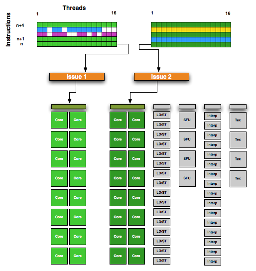
In order to facilitate superscalar operation, NVIDIA made some changes to both the warp scheduler and the dispatch unit for GF104. Each warp scheduler is now connected to 2 dispatch units, giving it the ability to dual-issue instructions. Along with its regular duties, a warp scheduler is now responsible for organizing its superscalar operation by analyzing the next instruction in its warp to determine if that instruction is ILP-safe, and whether there is an execution unit available to handle it. The result is that NVIDIA’s SMs now handle superscalar operation similar to that of a CPU, with the hardware taking the responsibility for dispatching parallel instructions. This in turn means that GF104 can execute a warp in a superscalar fashion for any code and including old CUDA code, allowing it to extract ILP out of old and new code alike. The GF104 compiler in NVIDIA’s drivers will try to organize code to better match GF104’s superscalar abilities, but it’s not critical to the ability.
NVIDIA GF104 SM - Note, more instructions in flight per SM vs. GF100
Ultimately superscalar execution serves 2 purposes on GF104: to allow it to issue instructions to the 3rd CUDA core block with only 2 warps in flight, and to improve overall efficiency. In a best-case scenario GF104 can utilize 4 of 7 execution units, while GF100 could only utilize 2 of 6 execution units.
The upside to this is that on average GF104 should be more efficient per clock than GF100, which is quite a remarkable feat. The downside to this is that now NVIDIA has a greater degree of best and worst case scenarios, as requiring superscalar execution to utilize the 3rd CUDA core block means that it’s harder to use that 3rd block than the previous 2. The ability to extract ILP from a warp will result in GF104’s compute abilities performing like a 384 CUDA core part some of the time, and like a 256 CUDA core part at other times. It will be less consistent, but on average faster than a pure 256 CUDA core part would be.
With the addition of superscalar abilities, GF104 marks the slow-but-steady merger of the CPU and the GPU. GF104 is now just a bit more CPU-like than GF100 was, a particularly interesting turn of events since we’re looking at a waterfall part and not a new architecture today.


93 Comments
View All Comments
threedeadfish - Monday, July 12, 2010 - link
I know you guys are all up in arms when a company releases information about up coming products, but you know that's information that can help a consumer.. I was looking for a card that was powerful enough while being quite and not using too much power. I ended up with a 5770 and I think it's a great product, however this the 460 offers 5830 performance at 5770 power and noise for only $30 more. I would have waited another week if I had any idea this was coming. You can't tell me nobody at Anandtech knew this was coming. Your anti-paper launch campain has a down site, it doesn't give consumers valuable information and as a result the video card I'll be using for the next couple years will be much less powerful then it would have been if the 465 artical just gave me a heads up, or just a little message saying hold off on $200 video card purchases something's coming. I only buy a new video card every few years please give me the information I need to make the best purchase. In this case waiting another week is what I should have done.notext - Monday, July 12, 2010 - link
If you notice, everyone put out their info on this card today. That is because an NDA. Even suggesting anything about this card without nVidia's permission is a quick way to guarantee you won't get future releases.Phate-13 - Monday, July 12, 2010 - link
Euhm, where can you find the "at 5770 power consumption"? The tables are quite clear that it uses 40-70Watts MORE under load then the 5770.And indeed, there is something called and NDA.
Phate-13 - Monday, July 12, 2010 - link
**** this. I want to be able to edit my posts.'something called AN NDA.'
Death666Angel - Thursday, July 15, 2010 - link
This is a review site, not a news or rumours site. If you are interested in the what the next couple of months bring from companies like Intel, AMD and nVidia, you need to start using sites like Fudzilla, that report hardware news and rumours.And trust me, there was plenty of information on the 460 being in the making and probably outperforming the 465 at a lower price point. :)
And if you regret the purchase of a 9 month old card because one that just got released has higher performance (20%-40%?), while using more electricity (20%), costs more (60% - 130€ to 210€ for the cheapest cards each), you are going to be a very sad PC buyer, because normally, a new product will be faster _and_ cheaper, while now it is just faster, but a hellovalot more expensive too. :-)
Lord 666 - Monday, July 12, 2010 - link
Definitely some details missing for a complete picture on this card.Lonyo - Monday, July 12, 2010 - link
There's more too.No real discussion of the reduction in polymorph engine to shader ratio, such as tessellation benchmarks (synthetic or otherwise).
Nothing on minimum frame rates (and anything which is put up uses the older 10.3 drivers for ATI).
In addition to the general compute performance benchmarks that you mention.
Nothing about CUDA games (e.g. Just Cause 2) comparing the GTX465 to the GTX460.
No consideration of ROP vs memory changes (i.e. is it memory bandwidth limited or is it purely the ROP reduction causing the performance hit on the 768MB card).
Maybe the cards didn't come out in time. Maybe everything, or more stuff at least, will be covered in Pt 2, but it is somewhat disappointing that so many things are totally missing.
Ryan Smith - Monday, July 12, 2010 - link
You hit the nail on the head with your comment on time. I actually have the data, but with the limited amount of time I had I wasn't able to write the analysis (most of my time was spent on better covering the architecture). That will be amended to the article later today, but for now you can see the raw graphs.http://images.anandtech.com/graphs/gtx460_07111017...
http://images.anandtech.com/graphs/gtx460_07111017...
http://images.anandtech.com/graphs/gtx460_07111017...
http://images.anandtech.com/graphs/gtx460_07111017...
Lonyo - Monday, July 12, 2010 - link
I hope I didn't come off as too harsh. I started writing and then towards the end realised it could be a time thing, and didn't go back to amend what I had written.After looking at most other sites, their reviews are sometimes even worse, covering only a very small handful of games.
Thanks for the early graphs, much appreciated. Shame NV didn't give more time for proper reviews.
jonny30 - Monday, July 12, 2010 - link
- maybe in your country my dear friend.......maybe there i tell you ;)- in my country is 300 you see.......300 as a price start i mean :)
- and for those 100 extra i buy another hdd for example, not another video card if you know what i mean
- so, maybe is worth for you, but for me to jump from 4870 to this......
- i am sorry, but it is not wort it........