The RV870 Story: AMD Showing up to the Fight
by Anand Lal Shimpi on February 14, 2010 12:00 AM EST- Posted in
- GPUs
Process vs. Architecture: The Difference Between ATI and NVIDIA
Ever since NV30 (GeForce FX), NVIDIA hasn’t been first to transition to any new manufacturing process. Instead of dedicating engineers to process technology, NVIDIA chooses to put more of its resources into architecture design. The flipside is true at ATI. ATI is much less afraid of new process nodes and thus devotes more engineering resources to manufacturing. Neither approach is the right one, they both have their tradeoffs.
NVIDIA’s approach means that on a mature process, it can execute frustratingly well. It also means that between major process boundaries (e.g. 55nm to 40nm), NVIDIA won’t be as competitive so it needs to spend more time to make its architecture more competitive. And you can do a lot with just architecture alone. Most of the effort put into RV770 was architecture and look at what it gave ATI compared to the RV670.
NVIDIA has historically believed it should let ATI take all of the risk jumping to a new process. Once the process is mature, NVIDIA would switch over. That’s great for NVIDIA, but it does mean that when it comes to jumping to a brand new process - ATI has more experience. Because ATI puts itself in this situation of having to jump to an unproven process earlier than its competitor, ATI has to dedicate more engineers to process technology in order to mitigate the risk.
In talking to me Carrell was quick to point out that moving between manufacturing processes is not a transition. A transition implies a smooth gradient from one technology to another. But moving between any major transistor nodes (e.g. 55nm to 45nm, not 90nm to 80nm) it’s less of a transition and more of a jump. You try to prepare for the jump, you try your best to land exactly where you want to, but once your feet leave the ground there’s very little to control where you end up.
Any process node jump involves a great deal of risk. The trick as a semiconductor manufacturer is how you minimize that risk.
At some point, both manufacturers have to build chips on a new process node otherwise they run the risk of becoming obsolete. If you’re more than one process generation behind, it’s game over for you. The question is, what type of chip do you build on a brand new process?
There are two schools of thought here: big jump or little jump. The size refers to the size of the chip you’re using in the jump.
Proponents of the little jump believe the following. In a new process, the defect density (number of defects per unit area on the wafer) isn’t very good. You’ll have a high number defects spread out all over the wafer. In order to minimize the impact of high defect density, you should use a little die.
If we have a wafer that has 100 defects across the surface of the wafer and can fit 1000 die on the wafer, the chance that any one die will be hit with a defect is only 10%.
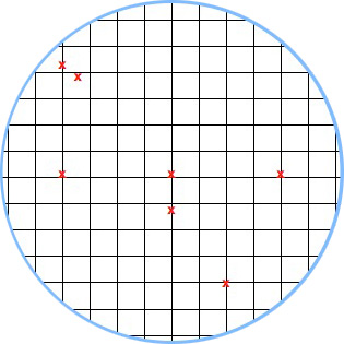
A hypothetical wafer with 7 defects and a small die. Individual die are less likely to be impacted by defects.
The big jump is naturally the opposite. You use a big die on the new process. Now instead of 1000 die sharing 100 defects, you might only have 200 die sharing 100 defects. If there’s an even distribution of defects (which isn’t how it works), the chance of a die being hit with a defect is now 50%.
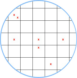
A hypothetical wafer with 7 defects and a large die.
Based on yields alone, there’s no reason you’d ever want to do a big jump. But there is good to be had from the big jump approach.
The obvious reason to do a big jump is if the things you’re going to be able to do by making huge chips (e.g. outperform the competition) will net you more revenue than if you had more of a smaller chip.
The not so obvious, but even more important reason to do a big jump is actually the reason most don’t like the big jump philosophy. Larger die are more likely to expose process problems because they will fail more often. With more opportunity to fail, you get more opportunity to see shortcomings in the process early on.
This is risky to your product, but it gives you a lot of learning that you can then use for future products based on the same process.


132 Comments
View All Comments
Stas - Sunday, February 14, 2010 - link
Awesome. Thanks!Adul - Sunday, February 14, 2010 - link
Really helps pass the time at work today. :) Keep it up.Btw when can we expect to see the new site launch?
aapocketz - Sunday, February 14, 2010 - link
[quote]I was convinced that ATI had embraced a new, refocused approach to GPU design, only to learn that they nearly threw out all of the learnings with the RV870. [/quote]It sounds like they have had some successes trying different techniques, but without stability in their production process it is hard to repeat success. I understand that they require constant innovation to stay competitive, but throwing out whole processes seems chaotic to me. I would like them to refine and improve successful processes rather than toss everything every time a new business guru is in charge.
Also half of their effort was all about openness and collaboration. The opening up of the PRS document so that "everyone was involved in the process" seems to clash with the hyper-secret groups where "AMD has since incorporated much of Carrell’s brand of information compartmentalization into how it handled other upcoming features." This seems like a recipe for disaster to me. Which is it, broad openness, collaboration and consesus; or secret teams that have no idea what the other teams are doing?
SuperGee - Sunday, February 14, 2010 - link
The story told us that they didn't know it will become a succes because these desision where made before RV770 release. So doing the high risk choice again. Wasn't a nobrainer. But a risky choice. We know that it turn out good now.mckirkus - Sunday, February 14, 2010 - link
It's kind of funny that you're not yet running one of these companies yet Anand.One of the reasons I check this site on a daily basis is because you also seem to also get the business side of the equation. It's downright refreshing to see someone bridging that gap. You pretty much saved the Vertex from self destruction. I'd like to see what interesting things you could build us if you put your mind to it.
deputc26 - Sunday, February 14, 2010 - link
Articles like these are what differentiate AnandTech from all the other sites out there. AnandTech goes from being one of the best review sites out there to something special.Beyond excellent, thanks Anand.
rickyv - Sunday, February 14, 2010 - link
As a loyal follower of your website for the past 15 years, I also felt that I just had to register and compliment you on an excellent article.With the rapid advancement of technology, it is very easy just to get caught up in the PR and marketing hype or focus only on the numbers game. We often lose sight of the fact that it is teams of dedicated people who make this possible. You have always had the ability to bring out the "human" side to this. I have not seen this on any other site nor in printed form (that is not an unashamedly PR marketing exercise).
Thanks for staying true to your roots by giving honest opinions of the technology that you review. The latest releases are not necessarily always the greatest (as much as the marketing departments would like us to believe :-) )
krish123 - Sunday, February 14, 2010 - link
After i read the article, I found that "Engine is running well and firing on all the cylinders", It can create better products in the future, I can trust and buy ATI products, hope they deliver better products in the future for my upgrade."Kudos to Anand for the excellent article".
By the way graphics card is a product, not just hardware, it has to work in tandem with the software, its better ATI put some more effort on the driver/software side and fix all the issues.
Krish
smartalec - Sunday, February 14, 2010 - link
"When companies like AMD and NVIDIA do a product the engineers don't know all of the answers, and the knowledge they do have isn't binary - it's probability, it's weight, it's guesses. Sometimes they guess right, and sometimes they guess very wrong. The best they can do is to all weigh in with their individual experiences and together come up with the best group of guesses to implement."I'm afraid this is how all engineering works. Project managers think that engineers can predict the future. That we know exactly how much time it'll take, and how much risk a given feature will bring.
We don't. There's a lot of educated guesses. Sometimes we're pleasantly surprised that what we thought was a tough problem wasn't. Sometimes we're the bearer of bad news-- something we assumed would be trivial wasn't.
My most frustrating issues aren't technical at all. I ask for 2000 hours, and are given 1000. Or are given 2 engineers instead of 3, and told-- figure out a way to get it done anyway, without impacting schedule.
Great article Anand.
mckirkus - Sunday, February 14, 2010 - link
Any decent project manager (I do software) reviews the risks up front with the engineers before building the project plan / timeline.The fact that most project managers don't really understand the products they manage is the rule not the exception. The problem is that great engineers don't always make great PMs. Having a good tech lead helps.