The RV870 Story: AMD Showing up to the Fight
by Anand Lal Shimpi on February 14, 2010 12:00 AM EST- Posted in
- GPUs
Process vs. Architecture: The Difference Between ATI and NVIDIA
Ever since NV30 (GeForce FX), NVIDIA hasn’t been first to transition to any new manufacturing process. Instead of dedicating engineers to process technology, NVIDIA chooses to put more of its resources into architecture design. The flipside is true at ATI. ATI is much less afraid of new process nodes and thus devotes more engineering resources to manufacturing. Neither approach is the right one, they both have their tradeoffs.
NVIDIA’s approach means that on a mature process, it can execute frustratingly well. It also means that between major process boundaries (e.g. 55nm to 40nm), NVIDIA won’t be as competitive so it needs to spend more time to make its architecture more competitive. And you can do a lot with just architecture alone. Most of the effort put into RV770 was architecture and look at what it gave ATI compared to the RV670.
NVIDIA has historically believed it should let ATI take all of the risk jumping to a new process. Once the process is mature, NVIDIA would switch over. That’s great for NVIDIA, but it does mean that when it comes to jumping to a brand new process - ATI has more experience. Because ATI puts itself in this situation of having to jump to an unproven process earlier than its competitor, ATI has to dedicate more engineers to process technology in order to mitigate the risk.
In talking to me Carrell was quick to point out that moving between manufacturing processes is not a transition. A transition implies a smooth gradient from one technology to another. But moving between any major transistor nodes (e.g. 55nm to 45nm, not 90nm to 80nm) it’s less of a transition and more of a jump. You try to prepare for the jump, you try your best to land exactly where you want to, but once your feet leave the ground there’s very little to control where you end up.
Any process node jump involves a great deal of risk. The trick as a semiconductor manufacturer is how you minimize that risk.
At some point, both manufacturers have to build chips on a new process node otherwise they run the risk of becoming obsolete. If you’re more than one process generation behind, it’s game over for you. The question is, what type of chip do you build on a brand new process?
There are two schools of thought here: big jump or little jump. The size refers to the size of the chip you’re using in the jump.
Proponents of the little jump believe the following. In a new process, the defect density (number of defects per unit area on the wafer) isn’t very good. You’ll have a high number defects spread out all over the wafer. In order to minimize the impact of high defect density, you should use a little die.
If we have a wafer that has 100 defects across the surface of the wafer and can fit 1000 die on the wafer, the chance that any one die will be hit with a defect is only 10%.
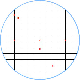
A hypothetical wafer with 7 defects and a small die. Individual die are less likely to be impacted by defects.
The big jump is naturally the opposite. You use a big die on the new process. Now instead of 1000 die sharing 100 defects, you might only have 200 die sharing 100 defects. If there’s an even distribution of defects (which isn’t how it works), the chance of a die being hit with a defect is now 50%.
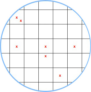
A hypothetical wafer with 7 defects and a large die.
Based on yields alone, there’s no reason you’d ever want to do a big jump. But there is good to be had from the big jump approach.
The obvious reason to do a big jump is if the things you’re going to be able to do by making huge chips (e.g. outperform the competition) will net you more revenue than if you had more of a smaller chip.
The not so obvious, but even more important reason to do a big jump is actually the reason most don’t like the big jump philosophy. Larger die are more likely to expose process problems because they will fail more often. With more opportunity to fail, you get more opportunity to see shortcomings in the process early on.
This is risky to your product, but it gives you a lot of learning that you can then use for future products based on the same process.


132 Comments
View All Comments
ImmortalZ - Monday, February 15, 2010 - link
Long time reader and lurker here.This article is one of the best I've read here - hell, it's one of the best I've ever read on any tech site. Reading about and getting perspective on what makes companies like ATI tick is great. Thank you and please, more!
tygrus - Sunday, February 14, 2010 - link
Sequences of numbers in a logical way are easier to remember than names. The RV500, RV600 .. makes order obvious. Using multiple names within a generation of chips are confusing and not memorable. They do not convey sequence or relative complexity.Can you ask if AMD are analysing current games/GPGPU and future games/GPGPU to identify possible areas for improvement or skip less useful proposed design changes. Like the Intel >2% gain for <1% cost.
Yakk - Sunday, February 14, 2010 - link
Excellent article! As I've read in a few other comments, this article (and one similar I'd read prior) made me register for the first time, even if I've been reading this site for many years.I could see why "Behind the scenes" articles can make certain companies nervous and others not, mostly based on their own "corporate culture" I'd think.
It was a very good read, and I'm sure every engineer who worked on any given generation on GPU's could have many stories to tell about tech challenges and baffling (at the time) corporate decisions. And also a manager's side of the work in navigating corporate red tape, working with people, while delivering something worthwhile as an end product is also a huge. Having a good manager (people) with a good subject knowledge (tech) is rare, then for Corp. Execs. to know they have one is MUCH rarer still...
If anyone at AMD/ATI read these comments, PLEASE look at the hardware division and try to implement changes to the software division to match their successes...
(btw been using nv cards almost exclusively since the TNT days, and just got a 5870 for the first time this month. ATI Hardware I'd give an "A+", Software... hmm, I'd give it a "C". Funny thing is nv is almost the exact opposite right now)
Perisphetic - Sunday, February 14, 2010 - link
Someone nominate this man for the Pulitzer Prize!As many have stated before, this is a fantastic article. It goes beyond extraordinary, exceptional and excellent. This has become my new benchmark for high quality computer industry related writing.
Thank you sir.
ritsu - Monday, February 15, 2010 - link
It's not exactly The Soul of a New Machine. But, fine article. It's nice to have a site willing to do this sort of work.shaggart5446 - Sunday, February 14, 2010 - link
very appreciative for this article im from ja but reading this make me file like ill go back to school thanks anand ur the best big up yeah man529th - Sunday, February 14, 2010 - link
The little knowledge I have about the business of making a graphics card, that it was Eyefinity that stunted the stability-growth of the 5xxx drivers by the allocation of resources of the software engineers to make Eyefinity work.chizow - Sunday, February 14, 2010 - link
I usually don't care much for these fluff/PR pieces but this one was pretty entertaining, probably because there was less coverage of what the PR/Marketing guys had to say and more emphasis on the designers and engineers. Carrell sounds like a very interesting guy and a real asset to AMD, they need more innovators like him leading their company and less media exposure from PR talking heads like Chris Hook. Almost tuned out when I saw that intro pic, thankfully the article shifted focus quickly.As for the article itself, among the many interesting points made in there, a few that caught my eye:
1) It sounds like some of the sacrifices made with RV870's die size help explain why it fell short of doubling RV770/790 in terms of performance scaling. Seems as if memory controllers might've also been cut as edge real estate was lost, and happen to be the most glaring case where RV870 specs weren't doubled with regard to RV770.
2) The whole cloak and dagger bit with EyeFinity was very amusing and certainly helps give these soulless tech giants some humanity and color.
3) Also with EyeFinity, I'd probably say Nvidia's solution will ultimately be better, as long as AMD continues to struggle with CrossFire EyeFinity support. It actually seems as if Nvidia is applying the same framebuffer splitting technology via PCIe/SLI link with their recently announced Optimus technology to Nvidia Surround, both of course lending technology from their Quadro line of cards.
4) The discussion about fabs/yields was also very interesting and helps shed some light on some of the differences between the strategies used by both companies in the past to present. AMD has always leveraged new process technologies in the past as soon as possible, Nvidia in the past has more closely followed Intel's Tick/Tock cadence of building high-end on mature processes and teething smaller chips on new processes. That clearly changed this time around on 40nm so it'll be interesting to see what AMD does going forward. I was surprised there wasn't any discussion about why AMD hasn't looked into GlobalFoundries as their GPU foundry.
SuperGee - Sunday, February 14, 2010 - link
nV eyeFinity counter solution is a fast software reaction wich is barly the same thing. You need SLI because one GPU can do only 2 active ports. That the main diference. So you depend on a more high-end platform. A SLI mobo PSU capable of feeding two Gcards. While ATI give yo 3 or 6 ou t of one GPU.nV can deliver something native in there next design. Equal and the possibility to be better at it. But we are still waiting for there DX11 parts. I wonder if they could slap a solution in the refresh or can do only wenn they introduce the new archtecture "GF200".
chizow - Monday, February 15, 2010 - link
Actually EyeFinity's current CF problems are most likely a software problem which is why Nvidia's solution is already superior from a flexibility and scalability standpoint. They've clearly worked out the kinks of running multiple GPUs to a single frame buffer and then redistributing portions of that framebuffer to different GPU outputs.AMD's solution seems to have problems because output on each individual GPU is only downstream atm, so while one GPU can send frame data to a primary GPU for CF, it seems secondary GPUs have problems receiving frame data to output portions of the frame.
Why I say Nvidia's solution is better overall is simply because the necessity of SLI will automatically decrease the chance of a poor gaming experience when gaming at triple resolutions, which is clearly a problem with some newer games and single-GPU EyeFinity. Also, if AMD was able to use multiple card display outputs, it would solve the problem of requiring a $100 active DP dongle for the 3rd output if a user doesn't have a DP capable monitor.