The RV870 Story: AMD Showing up to the Fight
by Anand Lal Shimpi on February 14, 2010 12:00 AM EST- Posted in
- GPUs
The Cost of Jumping to 40nm
This part of the story could almost stand on its own, but it directly impacts much of what happened with Cypress and the entire Evergreen stack that it’s worth talking about here.
By now you’ve most likely heard about issues with TSMC’s 40nm process. While the word is that the issues are finally over, poor yields and a slower than expected ramp lead to Cypress shortages last year and contributed to NVIDIA’s Fermi/GF100 delay. For the next couple of pages I want to talk about the move to 40nm and why it’s been so difficult.
The biggest issue with being a fabless semiconductor is that you have one more vendor to deal with when you’re trying to get out a new product. On top of dealing with memory companies, component manufacturers and folks who have IP you need, you also have to deal with a third party that’s going to actually make your chip. To make matters worse, every year or so, your foundry partner comes to you with a brand new process to use.
The pitch always goes the same way. This new process is usually a lot smaller, can run faster and uses less power. As with any company whose job it is to sell something, your foundry partner wants you to buy its latest and greatest as soon as possible. And as is usually the case in the PC industry, they want you to buy it before it's actually ready.
But have no fear. What normally happens is your foundry company will come to you with a list of design rules and hints. If you follow all of the guidelines, the foundry will guarantee that they can produce your chip and that it will work. In other words, do what we tell you to do, and your chip will yield.
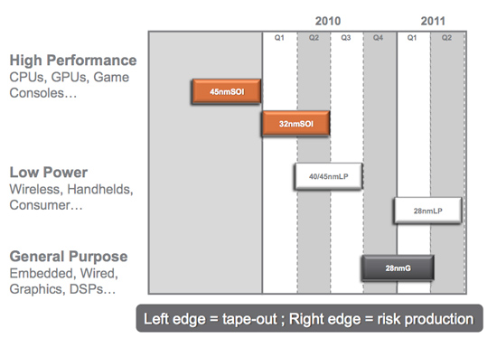
Global Foundries' 2010 - 2011 Manufacturing Roadmap
The problem is that if you follow every last one of these design rules and hints your chip won’t be any faster than it was on the older manufacturing process. Your yield will be about the same but your cost will be higher since you’ll bloat your design taking into account these “hints”.
Generally between process nodes the size of the wafer doesn’t change. We were at 200mm wafers for a while and now modern fabs use 300mm wafers. The transistor size does shrink however, so in theory you could fit more die on a wafer with each process shrink.
The problem is with any new process, the cost per wafer goes up. It’s a new process, most likely more complex, and thus the wafer cost is higher. If the wafer costs are 50% higher, then you need to fit at least 50% more die on each wafer in order to break even with your costs on the old process. In reality you actually need to fit more than 50% die per wafer on the new process because yields usually suck at the start. But if you follow the foundry’s guidelines to guarantee yield, you won’t even be close to breaking even.
The end result is you get zero benefit from moving to the new process. That’s not an option for anyone looking to actually use Moore’s Law to their advantage. Definitely not for a GPU company.
The solution is to have some very smart people in your company that can take these design rules and hints the foundry provides, and figure out which ones can be ignored, and ways to work around the others. This is an area where ATI and NVIDIA differ greatly.


132 Comments
View All Comments
ImmortalZ - Monday, February 15, 2010 - link
Long time reader and lurker here.This article is one of the best I've read here - hell, it's one of the best I've ever read on any tech site. Reading about and getting perspective on what makes companies like ATI tick is great. Thank you and please, more!
tygrus - Sunday, February 14, 2010 - link
Sequences of numbers in a logical way are easier to remember than names. The RV500, RV600 .. makes order obvious. Using multiple names within a generation of chips are confusing and not memorable. They do not convey sequence or relative complexity.Can you ask if AMD are analysing current games/GPGPU and future games/GPGPU to identify possible areas for improvement or skip less useful proposed design changes. Like the Intel >2% gain for <1% cost.
Yakk - Sunday, February 14, 2010 - link
Excellent article! As I've read in a few other comments, this article (and one similar I'd read prior) made me register for the first time, even if I've been reading this site for many years.I could see why "Behind the scenes" articles can make certain companies nervous and others not, mostly based on their own "corporate culture" I'd think.
It was a very good read, and I'm sure every engineer who worked on any given generation on GPU's could have many stories to tell about tech challenges and baffling (at the time) corporate decisions. And also a manager's side of the work in navigating corporate red tape, working with people, while delivering something worthwhile as an end product is also a huge. Having a good manager (people) with a good subject knowledge (tech) is rare, then for Corp. Execs. to know they have one is MUCH rarer still...
If anyone at AMD/ATI read these comments, PLEASE look at the hardware division and try to implement changes to the software division to match their successes...
(btw been using nv cards almost exclusively since the TNT days, and just got a 5870 for the first time this month. ATI Hardware I'd give an "A+", Software... hmm, I'd give it a "C". Funny thing is nv is almost the exact opposite right now)
Perisphetic - Sunday, February 14, 2010 - link
Someone nominate this man for the Pulitzer Prize!As many have stated before, this is a fantastic article. It goes beyond extraordinary, exceptional and excellent. This has become my new benchmark for high quality computer industry related writing.
Thank you sir.
ritsu - Monday, February 15, 2010 - link
It's not exactly The Soul of a New Machine. But, fine article. It's nice to have a site willing to do this sort of work.shaggart5446 - Sunday, February 14, 2010 - link
very appreciative for this article im from ja but reading this make me file like ill go back to school thanks anand ur the best big up yeah man529th - Sunday, February 14, 2010 - link
The little knowledge I have about the business of making a graphics card, that it was Eyefinity that stunted the stability-growth of the 5xxx drivers by the allocation of resources of the software engineers to make Eyefinity work.chizow - Sunday, February 14, 2010 - link
I usually don't care much for these fluff/PR pieces but this one was pretty entertaining, probably because there was less coverage of what the PR/Marketing guys had to say and more emphasis on the designers and engineers. Carrell sounds like a very interesting guy and a real asset to AMD, they need more innovators like him leading their company and less media exposure from PR talking heads like Chris Hook. Almost tuned out when I saw that intro pic, thankfully the article shifted focus quickly.As for the article itself, among the many interesting points made in there, a few that caught my eye:
1) It sounds like some of the sacrifices made with RV870's die size help explain why it fell short of doubling RV770/790 in terms of performance scaling. Seems as if memory controllers might've also been cut as edge real estate was lost, and happen to be the most glaring case where RV870 specs weren't doubled with regard to RV770.
2) The whole cloak and dagger bit with EyeFinity was very amusing and certainly helps give these soulless tech giants some humanity and color.
3) Also with EyeFinity, I'd probably say Nvidia's solution will ultimately be better, as long as AMD continues to struggle with CrossFire EyeFinity support. It actually seems as if Nvidia is applying the same framebuffer splitting technology via PCIe/SLI link with their recently announced Optimus technology to Nvidia Surround, both of course lending technology from their Quadro line of cards.
4) The discussion about fabs/yields was also very interesting and helps shed some light on some of the differences between the strategies used by both companies in the past to present. AMD has always leveraged new process technologies in the past as soon as possible, Nvidia in the past has more closely followed Intel's Tick/Tock cadence of building high-end on mature processes and teething smaller chips on new processes. That clearly changed this time around on 40nm so it'll be interesting to see what AMD does going forward. I was surprised there wasn't any discussion about why AMD hasn't looked into GlobalFoundries as their GPU foundry.
SuperGee - Sunday, February 14, 2010 - link
nV eyeFinity counter solution is a fast software reaction wich is barly the same thing. You need SLI because one GPU can do only 2 active ports. That the main diference. So you depend on a more high-end platform. A SLI mobo PSU capable of feeding two Gcards. While ATI give yo 3 or 6 ou t of one GPU.nV can deliver something native in there next design. Equal and the possibility to be better at it. But we are still waiting for there DX11 parts. I wonder if they could slap a solution in the refresh or can do only wenn they introduce the new archtecture "GF200".
chizow - Monday, February 15, 2010 - link
Actually EyeFinity's current CF problems are most likely a software problem which is why Nvidia's solution is already superior from a flexibility and scalability standpoint. They've clearly worked out the kinks of running multiple GPUs to a single frame buffer and then redistributing portions of that framebuffer to different GPU outputs.AMD's solution seems to have problems because output on each individual GPU is only downstream atm, so while one GPU can send frame data to a primary GPU for CF, it seems secondary GPUs have problems receiving frame data to output portions of the frame.
Why I say Nvidia's solution is better overall is simply because the necessity of SLI will automatically decrease the chance of a poor gaming experience when gaming at triple resolutions, which is clearly a problem with some newer games and single-GPU EyeFinity. Also, if AMD was able to use multiple card display outputs, it would solve the problem of requiring a $100 active DP dongle for the 3rd output if a user doesn't have a DP capable monitor.