AMD Reveals More Llano Details at ISSCC: 32nm, Power Gating, 4-cores, Turbo?
by Anand Lal Shimpi on February 8, 2010 12:00 AM EST- Posted in
- CPUs
After cashing Intel’s check and appearing more competitive than expected against Clarkdale 2010 is like a fresh start for AMD. The news gets better.
Late last year AMD said that before the end of 2010 it would be sampling its first APU (Accelerated Processing Unit) - codenamed Llano. Today AMD is announcing that the first Llano samples, built on Global Foundries 32nm high-k + metal gate, SOI process will be sampling to partners in the first half of this year.
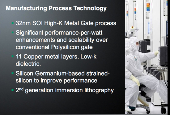
GF's 32nm SOI High-K + MG process will be used with Llano
For those not in the know, Llano is AMD’s first hybrid CPU-GPU with on-die graphics. The graphics core is a derivative of AMD’s DirectX 11 Evergreen lineup (the same lineage as the Radeon HD 5970, 5870, 5850, 5670, 5570, 5450, etc...).
Llano will go up against Sandy Bridge, which seems to have been pushed back to 2011 for volume availability according to Intel’s internal roadmaps. While Sandy Bridge will have graphics on-die, it will still only be DX10 class - AMD will have the feature-set advantage as far as graphics is concerned.
Llano's Features
Today we learn a bit more about the CPU side of Llano. The first chip will be a quad-core processor plus on-die graphics. Each core is Phenom II derived, but there’s no shared L3 cache. So Llano cores look a lot like Athlon II cores. I’m hearing that they may have some architectural tweaks, so performance could be better than present-day Athlon IIs.
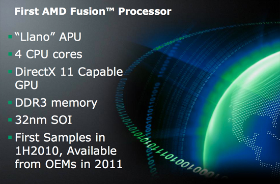
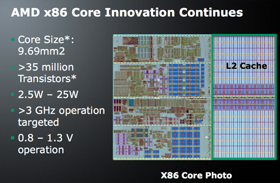
At 32nm each core (minus L2 cache) is only 9.69 mm^2 and is made up of over 35M transistors. Each core is paired with its own 1MB L2 cache, meaning the quad-core processor will have a total of 4MB of L2 on-die. AMD expects Llano to run at above 3GHz, which should be more than possible at 32nm given that we’re already at close to 3GHz with the 45nm Athlon II X4.
AMD’s First Power Gated CPU
With Nehalem Intel introduced power gating, a technique that allows a core to be near-completely powered down minimizing leakage current when inactive. This not only reduces idle power but it also enables Intel to use extra TDP to turbo up active cores.
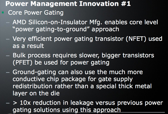
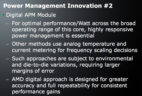
Llano uses power gating as well as a Digital APM Module. AMD doesn’t go into much detail on the digital APM module but I’m guessing we’ll see the same sort of turbo-like functionality out of Llano, including graphics turbo.
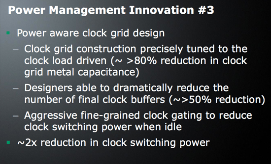
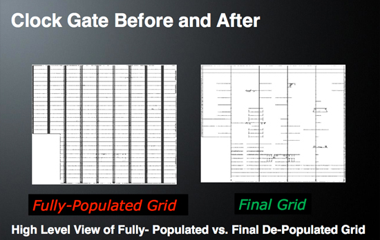
AMD also pointed out that Llano uses a “power aware clock grid design”. I couldn’t get much more information out of AMD on this one, other than its expecting a ~2x reduction in clock switching power. Simply distributing the clock to all parts of a modern day microprocessor can take up quite a bit of power, any improvements in efficiency there are very important.
I’ll keep digging to see if I can get any more details on this aspect of Llano.
Final Words
Llano will obviously require a new socket. All AMD is saying is that OEMs will be shipping systems in 2011. It’s unclear if we’ll see anything in the channel before then, but with sampling in the coming months it appears that AMD could be ready for Sandy Bridge when it arrives next year.
AMD isn’t qualifying its 2011 statement with an indication of what quarter to expect systems. Given that the first samples are going out now, I’d expect to see Llano sometime in the first half of 2011 but that’s purely conjecture on my part. Sandy Bridge is scheduled to ship in volume in the first quarter of 2011.
The big questions going forward are 1) how much AMD and Intel are going to scale up its graphics performance on these chips, and 2) how important DX11 support will be to the upcoming APU race.


58 Comments
View All Comments
Calin - Tuesday, February 9, 2010 - link
"that can emulate CISC commands quicker then native CISC CPU's"We already did. The last x86 processor that was entirely CISC (I too may be off base) is the 386. The 486 started using the pipeline (I think), Pentium used , and by the time of the Pentium M the micro-ops fusion appeared (CISC instructions are broken into RISC-like micro operations, and Pentium M could "fuse" together micro-ops to execute them in a single clock cycle - even if the micro-ops were from different x86 instructions).
As for emulating x86 with a different internal architecture, you should look at the Transmeta processors (which were very wide RISC-like internally, and ran x86 code thru some kind of interpreter)
qwertymac93 - Monday, February 8, 2010 - link
With DX11 support, comes support for the latest direct compute model. This support is meaningless for games as these "APU"s will be too weak to play games making use of it, but applications like video rendering might make use of this and accelerate encoding dramatically, we are already seeing this with the avivo video encoder, and 3rd party apps that use ati stream(and CUDA). the support of dx11 tells me this apu will be much more powerful then 3300/4200. with the launch of 5450, we saw that adding support for dx11 took up a very large amount of space, which is why 5450 has the same amount of stream units, despite using the much smaller 40nm process. I think dx11(and open cl) will play a bigger part in these new cpus and an igp with say, 120spu's would accelerate encoding(and general fp performance i bet) dramatically. all of this makes sense as bulldozer will have half as many FP units as integer, the igp will have to pick up the slack.Griswold - Tuesday, February 9, 2010 - link
Its not meaningless per say because that GPU could be used to calculate physics via direct compute and leave the horsepower of the discrete card to the rendering of graphics.ExarKun333 - Monday, February 8, 2010 - link
Let's see some benchmarks, otherwise this is just PR stuff I could get from AMD.com...Basilisk - Monday, February 8, 2010 - link
to me why a new socket is necessitated. I'm not doubting you, and I can think of ways that on-chip graphics might benefit from a few pins, but I'd appreciate a clarification.Jellodyne - Tuesday, February 9, 2010 - link
I dunno why the completed frames could be sent out on the HT bus -- a relatively simple HT-to-video out device, either standalone or in the southbridge, could unpack them to DVI or a DAC if you're going to a VGA out. And the MB would work without cpu with onboard video -- the vid outs just wouldn't function.Calin - Tuesday, February 9, 2010 - link
I don't know how much of the integrated graphics are on the microprocessor. However, to output a high definition image (1920 by 1080 at 60 Hz, 16 millions colours) one needs to send out about 480 MBps of data (8 MBytes for a frame, times 60 frames a second).Now, the processor has quite a bit of memory bandwidth, and quite a bit of HyperTransport bandwidth - but it will be eaten into by the need to use some of it for GPU memory access (remember that current generation graphic cards use tens of GBps of memory bandwidth, and are in some cases limited by memory bandwidth). Contrasting this, CPUs hardly go over 10 GBps memory bandwidth.
These being said, I think the processor will have direct video output, and for this reason it needs some more dedicated pins (nine for VGA, maybe another ten for DVI, and some others of those pins for HDMI, DisplayPort, whatever else). This will make the mainboards cheaper and easier to build, would allow the use of existing north/south bridges and so on.
JKflipflop98 - Wednesday, February 10, 2010 - link
We try to keep as few pins on the processor as needed. I would imagine there's only 8-10 video out pins that will need to be ran though a conversion chip of some sort to convert to monitor output. The CPU die itself is incapable of handling the +/- 5V needed to power your DVI connection.FaaR - Tuesday, February 9, 2010 - link
No reason to add piles and piles of extra pins to the CPU to support the current mess of analog and digital interconnects, as well as waste die space on DACs, TDMS transmitters and so on when all of that belongs much more in the chipset.Consider AMDs current infatuation with multi-monitor support. Just how MANY pins would you like AMD to add to support 3+ monitors? It'd require dozens. You pack all that shit into the chipset instead and voila - you can support virtually as many monitors as you like. The hypertransport bus will be virtually unused with on-die graphics (save for some intermittent disk and network I/O which is marginal compared to the total bandwidth of the interface), it could support an almost "unlimited" number of outputs, or at least as many as the system has room for on the backplate. :)
Not sure how you figure monitor outputs coming from the CPU would be "cheaper" or "easier to build" than them coming from the chipset. Seems about the same from my perspective.
GeorgeH - Monday, February 8, 2010 - link
That threw me as well; Intel doesn't need a new socket for P55 vs H55, so why would AMD?