At this year’s Consumer Electronics Show, NVIDIA had several things going on. In a public press conference they announced 3D Vision Surround and Tegra 2, while on the showfloor they had products o’plenty, including a GF100 setup showcasing 3D Vision Surround.
But if you’re here, then what you’re most interested in is what wasn’t talked about in public, and that was GF100. With the Fermi-based GF100 GPU finally in full production, NVIDIA was ready to talk to the press about the rest of GF100, and at the tail-end of CES we got our first look at GF100’s gaming abilities, along with a hands-on look at some unknown GF100 products in action. The message NVIDIA was trying to send: GF100 is going to be here soon, and it’s going to be fast.
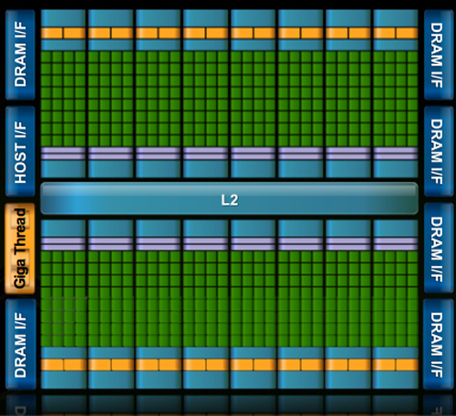
Fermi/GF100 as announced in September of 2009
Before we get too far ahead of ourselves though, let’s talk about what we know and what we don’t know.
During CES, NVIDIA held deep dive sessions for the hardware press. At these deep dives, NVIDIA focused on 3 things: Discussing GF100’s architecture as is relevant for a gaming/consumer GPU, discussing their developer relations program (including the infamous Batman: Arkham Asylum anti-aliasing situation), and finally demonstrating GF100 in action on some games and some productivity applications.
Many of you have likely already seen the demos, as videos of what we saw have already been on YouTube for a few days now. What you haven’t seen and what we’ll be focusing on today, is what we’ve learned about GF100 as a gaming GPU. We now know everything about what makes GF100 tick, and we’re going to share it all with you.
With that said, while NVIDIA is showing off GF100, they aren’t showing off the final products. As such we can talk about the GPU, but we don’t know anything about the final cards. All of that will be announced at a later time – and no, we don’t know that either. In short, here’s what we still don’t know and will not be able to cover today:
- Die size
- What cards will be made from the GF100
- Clock speeds
- Power usage (we only know that it’s more than GT200)
- Pricing
- Performance
At this point the final products and pricing are going to heavily depend on what the final GF100 chips are like. The clockspeeds NVIDIA can get away with will determine power usage and performance, and by extension of that, pricing. Make no mistake though, NVIDIA is clearly aiming to be faster than AMD’s Radeon HD 5870, so form your expectations accordingly.
For performance in particular, we have seen one benchmark: Far Cry 2, running the Ranch Small demo, with NVIDIA running it on both their unnamed GF100 card and a GTX285. The GF100 card was faster (84fps vs. 50fps), but as Ranch Small is a semi-randomized benchmark (certain objects are in some runs and not others) and we’ve seen Far Cry 2 to be CPU-limited in other situations, we don’t put much faith in this specific benchmark. When it comes to performance, we’re content to wait until we can test GF100 cards ourselves.
With that out of the way, let’s get started on GF100.


115 Comments
View All Comments
deputc26 - Monday, January 18, 2010 - link
This may be the most dragged-out launch ever.Vinb2k10 - Monday, January 18, 2010 - link
Try the Chevy Volt.SlyNine - Monday, January 18, 2010 - link
I just hope it doesn't end up being a 5800GT. the 5870 is a great card, but it's not exactly the ATI 9700pro of its time.SlyNine - Monday, January 18, 2010 - link
My bad, 5800 ultra.Ryan Smith - Monday, January 18, 2010 - link
Working on the images now guys.