P55 Overclocking Showdown - ASUS, Gigabyte, and EVGA at the OC Corral (Page 6 Updated)
by Rajinder Gill on November 6, 2009 12:00 PM EST- Posted in
- Motherboards
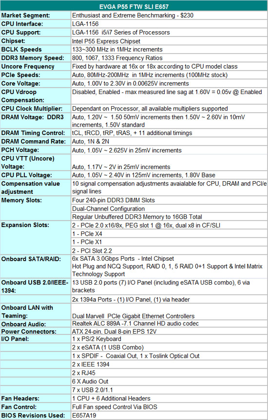
EVGA P55 FTW SLI
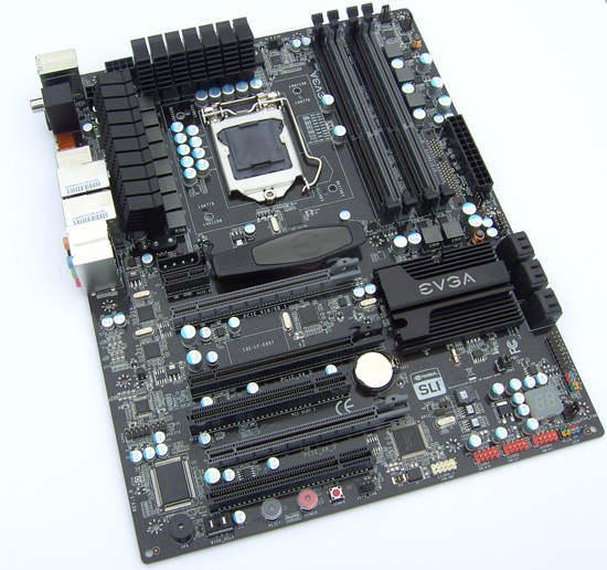
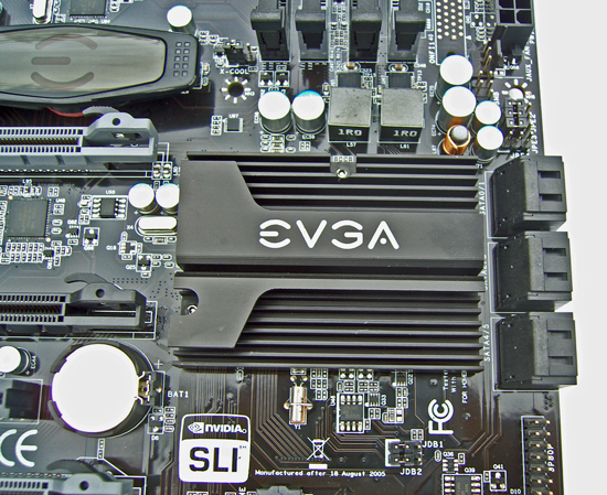
The EVGA E657 board is a little lighter in terms of onboard peripheral count when compared to the Gigabyte UD6 (additional SATA ports and software) and ASUS ROG, although the E657 FTW touts additional dedicated hardware features for overclocking (cold boot workarounds and 10 dedicated ICs allow for fine control of signal line compensation to the CPU, PCI/e and memory). CPU Power is supplied by a 12-phase, 600W capable PWM circuit, more than overkill on this platform.
A total of 7 fan headers are placed in accessible locations across the motherboard, with full fan speed control offered via BIOS. PWM cooling is catered for by two separate aluminium heat sinks that are attached to the board with screw fittings.
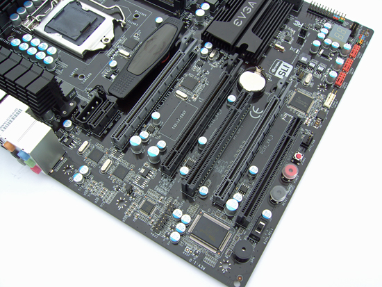
Starting at the top, expansion slot layout is comprised of PCI/eX1, PCI/e x16 (x8 if PEG slot 3 is occupied), PCI/e x4, PCI slot 1, PCI/e x8 and finally PCI slot 2.
Slot layout ensures that a PCI slot and the PCI/e x1 slots are always available/. The PCI/e x4 slot is also accessible when the primary PEG slot is occupied, although a double slot GPU will mean spacing will be tight. Underneath the last PCI slot, we find power, reset and CMOS clear buttons.
A three way slider switch is also provided allowing user selection of 3 separate BIOS IC’s. This allows flashing 3 different BIOS files, and also adds a good level of security in the instance of a corrupt BIOS flash. Along the bottom edge of the E657 we find a fan header, single IEEE-1394a connector, and three USB headers.
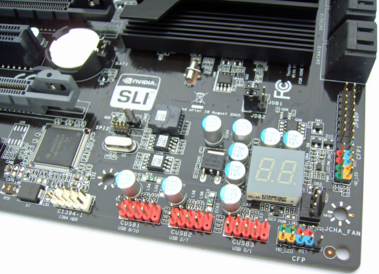
A hex post code display is placed in the lower right corner of the board and over to the left we find 3 BIOS IC’s, one of which is placed within a socket allowing removal if a swap out is required. The CFP1 connector is the EVGA OCP PCB panel connector which allows for on the fly changes 0.1V boost functions to CPU Core and VTT as well as a post code reader and power, reset and CMOS clear buttons.
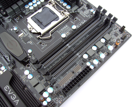
PCI/e disable and X-Cool jumpers are located underneath the DIMM slots. Memory power is supplied by a three phase controller supporting switching speeds up to 640KHz. Voltage measurement pads for all primary rails are located above the DIMM slots ensuring unhindered access in open test bed setups.
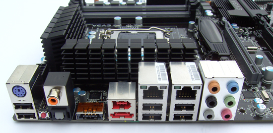
On the rear I/O panel we find, 1 x PS2, 7 X USB (1 SATA combo), 1x S/PDIF, 1x Optical, 1 x 1394, 2x RJ45 LAN and 6 x audio connectors. A CMOS reset button is located between the PS2 and S/SPDIF connectors for easy CMOS clear events with the board in a case.
Worthy of mention here is the addition of boot up voltage settings for VTT and processor Core allowing users to cold boot processors at high frequencies by applying a lower voltage during initial post.
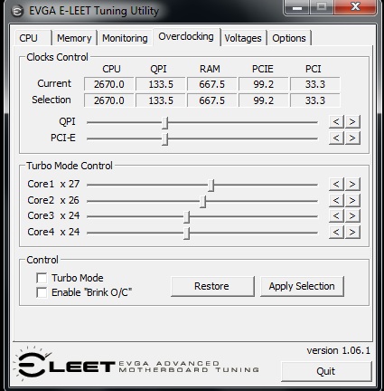
EVGA’s spin of a OS level overclocking tool know as E-LEET is also available for the P55 platform and is still the de-facto standard for all other OS overclocking tools to be judged against. ASUS’ new Connect software is close but simplicity rules here. The E-LEET GUI is remarkably compact and well laid out, offering voltage control, temperature/voltage readings, bus speed control, CPU-Z validation, quick load profiles and the ability to stop polling the SMbus. The latter feature is useful if you’d like to change processor speeds on-the-fly while minimizing the impact of having an application running in the background during a benchmark.


52 Comments
View All Comments
michael19 - Friday, November 6, 2009 - link
"Our test sample arrived with the revised Foxconn socket.."how can we tell if we have the revised foxconn socket as opposed to the defective version?
Rajinder Gill - Friday, November 6, 2009 - link
No idea at this point. Only Foxconn seem to know what it is they changed in the June revision.michael19 - Friday, November 6, 2009 - link
Or perhaps a side by side picture would show us some noticeable visual differences, possibly..cmdrdredd - Friday, November 6, 2009 - link
How come the Asus board is left out of the final few notes and tests? It's in the 3DMark and SuperPi scores etc, but there's individual pages dedicated to the other boards...Samus - Monday, November 9, 2009 - link
probably because it failed mid-testingAstroGuardian - Wednesday, November 11, 2009 - link
It's socket burned as a result of not so extreme overclock. It's not ASUS fault, it's Foxconn's faulty socketRajinder Gill - Friday, November 6, 2009 - link
Hi,The ASUS board died before I could complete the 750 retail CPU testing. We just got a new board last week so I will possibly update when that arrives here.
later
Raja
cmdrdredd - Friday, November 6, 2009 - link
lol well, a dead board spells trouble anyway IMO. Unless something drastic was done to it (extreme overclock for example).michael19 - Friday, November 6, 2009 - link
OK, thank you. Would the numbers on the backplate give us any indication? Is there any consistent difference in the numbers printed on the backplate from the old burnt out sockets to the new ones you have now?Corsairs - Friday, November 6, 2009 - link
I'd love to see this board compared to the group reviewed here.