P55 Overclocking Showdown - ASUS, Gigabyte, and EVGA at the OC Corral (Page 6 Updated)
by Rajinder Gill on November 6, 2009 12:00 PM EST- Posted in
- Motherboards
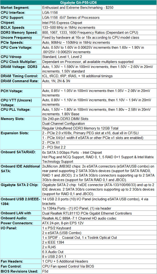
Gigabyte GA-P55-UD6
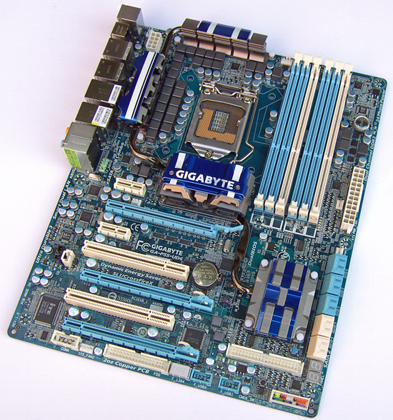
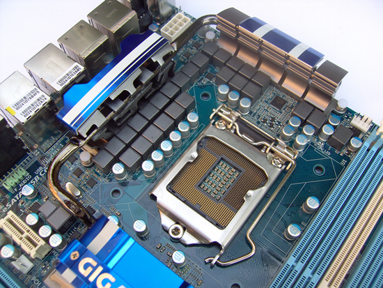
Gigabyte’s top end offering comes in at $250 and touts their answer to competing boards as having ’24-Phase’ PWM circuit (using a multiplexed ISL6336 6 phase controller). Onboard cooling of the MOSFET area, Intel P55 PCH , and Gigabyte SATA chips is provided by a heatsink/heatpipe setup connecting all three areas together. The PCH portion of the heat sink is attached with screws while the PWM MOSFETs and Gigabyte SATA chip fittings are of push-pin type (screw fittings are our favorites).
A total of 6 fan headers are available (two of which are 4 pin). Our retail sample came with a Foxconn CPU socket, although Gigabyte is moving to LOTES sockets on their upper end boards after hearing of the problems some users have experienced with the early Foxconn sockets.
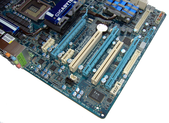
Expansion slot layout is identical to the ASUS Maximus III ROG, which is a good thing in our opinion. Starting at the top, we’ve got a PCI/eX1 slot, followed by PCI/e X16 and then another CPI/eX1 slot immediately beneath. Moving down, we get a PCI slot, the second PEG slot (running at 8X) followed by the second PCI slot and finally the last 16x mechanical PCI/e slot (running at 4x width). Slot layout is good, allowing for a variety of peripheral cards to be used in tandem. Underneath the last PCI/e slot at the lower edge of the board, we have 1XCOM port, 1XFDD, 1X1394 and 2 x USB headers.
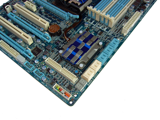
The lower right hand corner of the Gigabyte P55 UD6 is home to 10 right angled SATA ports (6 X Intel ICH10R and 4 Gigabyte SATA). A Hex post code reader is also included for debugging purposes. Just behind the Hex display, we’ve got CMOS clear and a reset switch for open test bed users. Finally an IDE port is provided for legacy drive users.
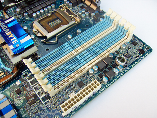
We’re a tad bemused at the presence of 6 DIMM slots on a P55 motherboard when the processors are dual channel only when run without buffered DIMMS. Oddly enough, the extra slots are for running single sided modules in dual channel interleaved mode over 6 slots. We’re not sure if this is a wise move at all because most users have moved over to double density 2GB modules which are priced attractively and capable of overclocking to high bandwidth due to advancements in memory IC design and memory controller design over previous platforms.
An onboard power button is placed very conveniently at the upper right edge of the board allowing for easy access in open test bed setups. Unfortunately, unlike the ASUS and EVGA boards, Gigabyte does not provide any voltage measurement pads for digital multimeters which can make the board a little tricky to get to grips with if you’re benchmarking under LN2.
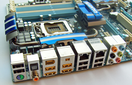
The rear panel is home to 1 x PS2, 8 x USB (2 SATA combo), 2 x1394, 1 x coaxial S/PDIF, 1 x TOSLINK optical, 2X RJ45 LAN ports and finally 6 audio output jacks. The presence of a rear CMOS clear switch would have been welcome for ease of access but is unfortunately missing. This leaves users with PC cases having to pull the side panel off their case if BIOS does not recover from a failed overclock.
Gigabyte’s Easy Tune software is bundled with the motherboard, and allows for easy access to all primary voltage rails as well as bus speed manipulation and fan control options.
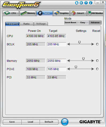
We found the Easy Tune software to be easy to use and to present a light enough system load to allow for unhindered overclocking. The only thing that would perhaps bolster Easy Tune would be the addition of hot keys with fast load profiles allowing for on the fly bus speed changes to maximize benchmark scoring potential. Other than that it’s a well rounded and easy to use tool.


52 Comments
View All Comments
michael19 - Friday, November 6, 2009 - link
"Our test sample arrived with the revised Foxconn socket.."how can we tell if we have the revised foxconn socket as opposed to the defective version?
Rajinder Gill - Friday, November 6, 2009 - link
No idea at this point. Only Foxconn seem to know what it is they changed in the June revision.michael19 - Friday, November 6, 2009 - link
Or perhaps a side by side picture would show us some noticeable visual differences, possibly..cmdrdredd - Friday, November 6, 2009 - link
How come the Asus board is left out of the final few notes and tests? It's in the 3DMark and SuperPi scores etc, but there's individual pages dedicated to the other boards...Samus - Monday, November 9, 2009 - link
probably because it failed mid-testingAstroGuardian - Wednesday, November 11, 2009 - link
It's socket burned as a result of not so extreme overclock. It's not ASUS fault, it's Foxconn's faulty socketRajinder Gill - Friday, November 6, 2009 - link
Hi,The ASUS board died before I could complete the 750 retail CPU testing. We just got a new board last week so I will possibly update when that arrives here.
later
Raja
cmdrdredd - Friday, November 6, 2009 - link
lol well, a dead board spells trouble anyway IMO. Unless something drastic was done to it (extreme overclock for example).michael19 - Friday, November 6, 2009 - link
OK, thank you. Would the numbers on the backplate give us any indication? Is there any consistent difference in the numbers printed on the backplate from the old burnt out sockets to the new ones you have now?Corsairs - Friday, November 6, 2009 - link
I'd love to see this board compared to the group reviewed here.