P55 Overclocking Showdown - ASUS, Gigabyte, and EVGA at the OC Corral (Page 6 Updated)
by Rajinder Gill on November 6, 2009 12:00 PM EST- Posted in
- Motherboards
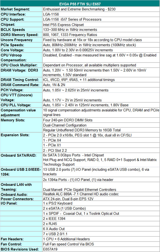
EVGA P55 FTW SLI
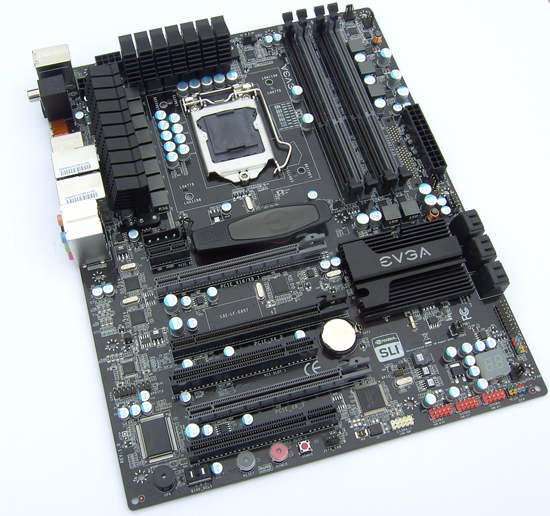
The EVGA E657 board is a little lighter in terms of onboard peripheral count when compared to the Gigabyte UD6 (additional SATA ports and software) and ASUS ROG, although the E657 FTW touts additional dedicated hardware features for overclocking (cold boot workarounds and 10 dedicated ICs allow for fine control of signal line compensation to the CPU, PCI/e and memory). CPU Power is supplied by a 12-phase, 600W capable PWM circuit, more than overkill on this platform.
A total of 7 fan headers are placed in accessible locations across the motherboard, with full fan speed control offered via BIOS. PWM cooling is catered for by two separate aluminium heat sinks that are attached to the board with screw fittings.
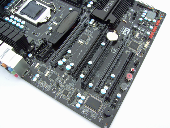
Starting at the top, expansion slot layout is comprised of PCI/eX1, PCI/e x16 (x8 if PEG slot 3 is occupied), PCI/e x4, PCI slot 1, PCI/e x8 and finally PCI slot 2.
Slot layout ensures that a PCI slot and the PCI/e x1 slots are always available/. The PCI/e x4 slot is also accessible when the primary PEG slot is occupied, although a double slot GPU will mean spacing will be tight. Underneath the last PCI slot, we find power, reset and CMOS clear buttons.
A three way slider switch is also provided allowing user selection of 3 separate BIOS IC’s. This allows flashing 3 different BIOS files, and also adds a good level of security in the instance of a corrupt BIOS flash. Along the bottom edge of the E657 we find a fan header, single IEEE-1394a connector, and three USB headers.
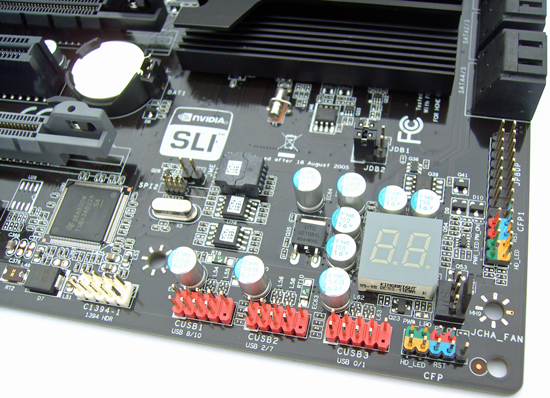
A hex post code display is placed in the lower right corner of the board and over to the left we find 3 BIOS IC’s, one of which is placed within a socket allowing removal if a swap out is required. The CFP1 connector is the EVGA OCP PCB panel connector which allows for on the fly changes 0.1V boost functions to CPU Core and VTT as well as a post code reader and power, reset and CMOS clear buttons.
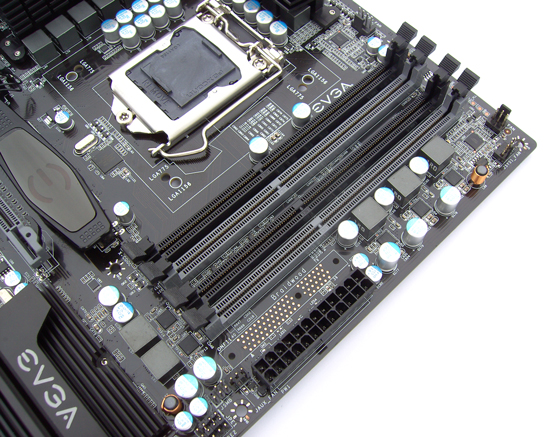
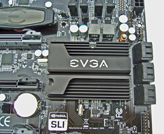
PCI/e disable and X-Cool jumpers are located underneath the DIMM slots. Memory power is supplied by a three phase controller supporting switching speeds up to 640KHz. Voltage measurement pads for all primary rails are located above the DIMM slots ensuring unhindered access in open test bed setups.
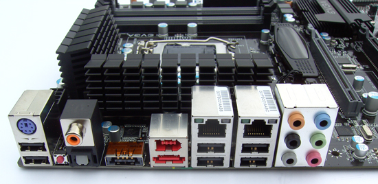
On the rear I/O panel we find, 1 x PS2, 7 X USB (1 SATA combo), 1x S/PDIF, 1x Optical, 1 x 1394, 2x RJ45 LAN and 6 x audio connectors. A CMOS reset button is located between the PS2 and S/SPDIF connectors for easy CMOS clear events with the board in a case.
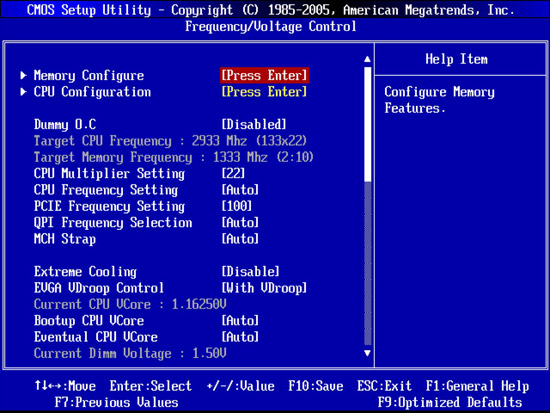
Worthy of mention here is the addition of boot up voltage settings for VTT and processor Core allowing users to cold boot processors at high frequencies by applying a lower voltage during initial post.
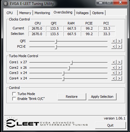
EVGA’s spin of a OS level overclocking tool know as E-LEET is also available for the P55 platform and is still the de-facto standard for all other OS overclocking tools to be judged against. ASUS’ new Connect software is close but simplicity rules here. The E-LEET GUI is remarkably compact and well laid out, offering voltage control, temperature/voltage readings, bus speed control, CPU-Z validation, quick load profiles and the ability to stop polling the SMbus. The latter feature is useful if you’d like to change processor speeds on-the-fly while minimizing the impact of having an application running in the background during a benchmark.


52 Comments
View All Comments
Rajinder Gill - Saturday, November 7, 2009 - link
For max BCLK testingPCI/e speeds were increased (where required) to 115MHz or so (the highest the CPU's I had could run were between 115-118MHz). I tried changes to RTL, memory dividers and all voltages were also changed. Subtiming ranges were shifted out to near maximums to see if that helped and also matched between the best and worst boards in the tests just to make sure something was not creating a hurdle.regards
Raja
dingetje - Friday, November 6, 2009 - link
wow the p55 platform is totally screwd if this problem persists...any overclocker still oc'ing the hell out of their p55 must be either brave, rich or (michael jackson voice on:) ignoraaaantdingetje - Friday, November 6, 2009 - link
oops, this was supposed to be a comment, not a reply...damn UI :Pdingetje - Friday, November 6, 2009 - link
now if we could only edit our posts I would so happypetergab - Friday, November 6, 2009 - link
What about any MSI boards? I know they may not count to the "extreme" OC but I think they should have a representative in such reviews.Rajinder Gill - Friday, November 6, 2009 - link
The MSI board was due to be included but left out becasue of CPU damage that occurred during the socket burnouts. This left no real way of cross comparing the prior results with the MSI boards abilities on the same CPU. At that point I decided to run with what I had at the time rather than starting afresh thus delaying the article even further.regards
Raja
spiderbutt - Friday, November 6, 2009 - link
Are you planning to include the MSI boards at a later date? I am curious to see how they compare to the other boards.Thanks for your hard work Raja it is appreciated!
Rajinder Gill - Friday, November 6, 2009 - link
Hi,There will be some MSI P55 board reviews coming, although those were planned in more typical usage scenarios. I guess what I can do is use a different CPU in the E657 EVGA board for cross compare to any high-end P55 MSI offering we review to see how things stack up.
regards
Raja
1stguess - Friday, November 6, 2009 - link
Wow. This is a bold article. Does anyone dare OC their P55 setup? Madness.jav6454 - Friday, November 6, 2009 - link
I've been looking at these P55 boards and somehow I always thought high of the EVGA. However these results have proven my gut feeling right.Bad thing of the EVGA boards is sometimes their higher price tag.