P55 Overclocking Showdown - ASUS, Gigabyte, and EVGA at the OC Corral (Page 6 Updated)
by Rajinder Gill on November 6, 2009 12:00 PM EST- Posted in
- Motherboards
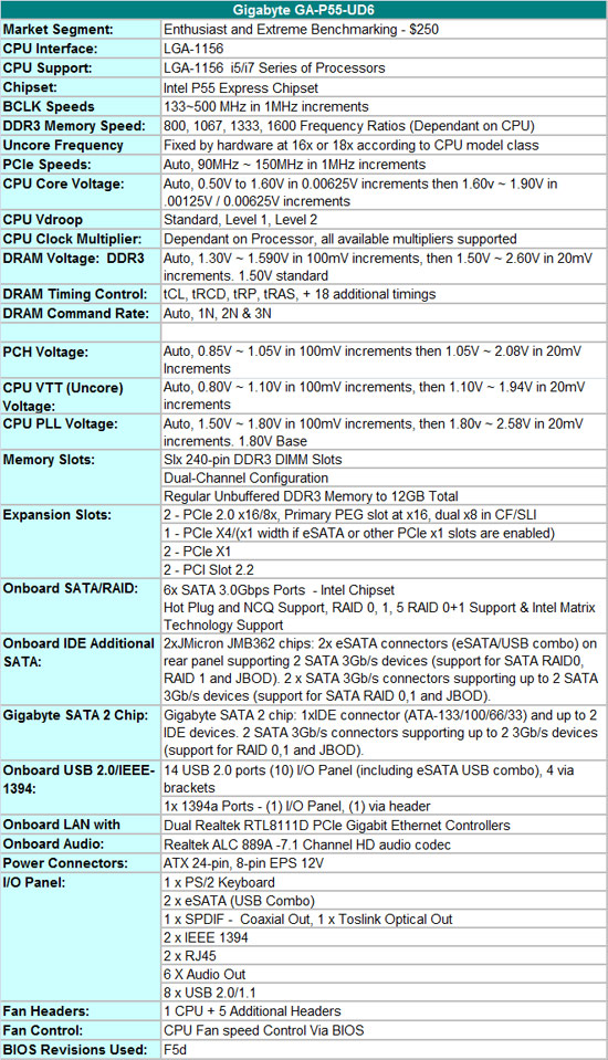
Gigabyte GA-P55-UD6
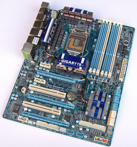
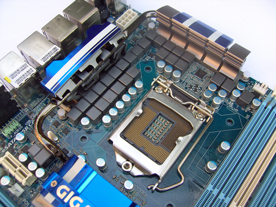
Gigabyte’s top end offering comes in at $250 and touts their answer to competing boards as having ’24-Phase’ PWM circuit (using a multiplexed ISL6336 6 phase controller). Onboard cooling of the MOSFET area, Intel P55 PCH , and Gigabyte SATA chips is provided by a heatsink/heatpipe setup connecting all three areas together. The PCH portion of the heat sink is attached with screws while the PWM MOSFETs and Gigabyte SATA chip fittings are of push-pin type (screw fittings are our favorites).
A total of 6 fan headers are available (two of which are 4 pin). Our retail sample came with a Foxconn CPU socket, although Gigabyte is moving to LOTES sockets on their upper end boards after hearing of the problems some users have experienced with the early Foxconn sockets.
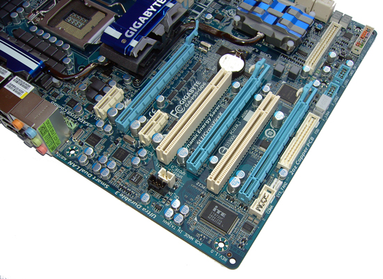
Expansion slot layout is identical to the ASUS Maximus III ROG, which is a good thing in our opinion. Starting at the top, we’ve got a PCI/eX1 slot, followed by PCI/e X16 and then another CPI/eX1 slot immediately beneath. Moving down, we get a PCI slot, the second PEG slot (running at 8X) followed by the second PCI slot and finally the last 16x mechanical PCI/e slot (running at 4x width). Slot layout is good, allowing for a variety of peripheral cards to be used in tandem. Underneath the last PCI/e slot at the lower edge of the board, we have 1XCOM port, 1XFDD, 1X1394 and 2 x USB headers.
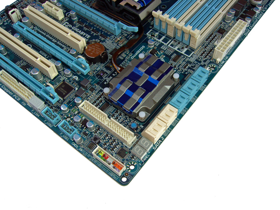
The lower right hand corner of the Gigabyte P55 UD6 is home to 10 right angled SATA ports (6 X Intel ICH10R and 4 Gigabyte SATA). A Hex post code reader is also included for debugging purposes. Just behind the Hex display, we’ve got CMOS clear and a reset switch for open test bed users. Finally an IDE port is provided for legacy drive users.
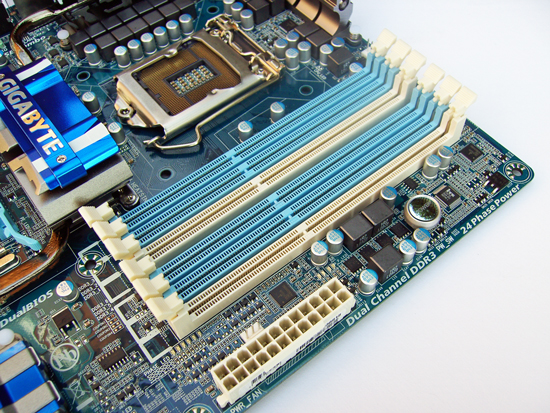
We’re a tad bemused at the presence of 6 DIMM slots on a P55 motherboard when the processors are dual channel only when run without buffered DIMMS. Oddly enough, the extra slots are for running single sided modules in dual channel interleaved mode over 6 slots. We’re not sure if this is a wise move at all because most users have moved over to double density 2GB modules which are priced attractively and capable of overclocking to high bandwidth due to advancements in memory IC design and memory controller design over previous platforms.
An onboard power button is placed very conveniently at the upper right edge of the board allowing for easy access in open test bed setups. Unfortunately, unlike the ASUS and EVGA boards, Gigabyte does not provide any voltage measurement pads for digital multimeters which can make the board a little tricky to get to grips with if you’re benchmarking under LN2.
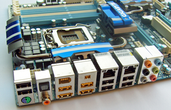
The rear panel is home to 1 x PS2, 8 x USB (2 SATA combo), 2 x1394, 1 x coaxial S/PDIF, 1 x TOSLINK optical, 2X RJ45 LAN ports and finally 6 audio output jacks. The presence of a rear CMOS clear switch would have been welcome for ease of access but is unfortunately missing. This leaves users with PC cases having to pull the side panel off their case if BIOS does not recover from a failed overclock.
Gigabyte’s Easy Tune software is bundled with the motherboard, and allows for easy access to all primary voltage rails as well as bus speed manipulation and fan control options.
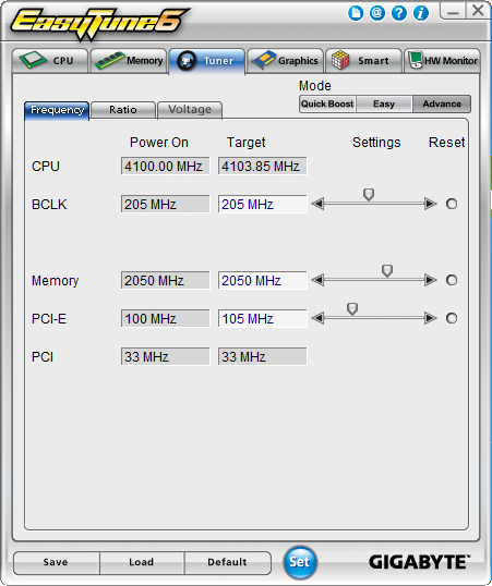
We found the Easy Tune software to be easy to use and to present a light enough system load to allow for unhindered overclocking. The only thing that would perhaps bolster Easy Tune would be the addition of hot keys with fast load profiles allowing for on the fly bus speed changes to maximize benchmark scoring potential. Other than that it’s a well rounded and easy to use tool.


52 Comments
View All Comments
yyrkoon - Saturday, November 7, 2009 - link
Ok, sorry for the rude comments. But the main reason why this perturbed me, is that something similar happened to a company that I did like a few years back. They lost a lot of revenue because of the situation( and then left the market altogether; yeah . . . guess who ). With that said, I am glad that you guys reported this issue, because at that time, I was seriously considering the board afflicted. Then, I could even go as far back as the terrible capacitors used by many builders, which also caused bad reviews(and feeling from loyal customers)from many reviewers. You would think these companies would learn eventually. Of course, at the time, the builders had no idea these capacitors were going to ruin long term stability ( or maybe they did ? ). Then even in some cases long term was not an issue, because short term stability suffered as well.So, for now on, I suppose I will just have to remember that highly OCable motherboards,are not really dependable for 24/7 operation, and then keep my "mouth" shut :)
I am glad to see one of you does have something from MSI. Now if only the other players would get something out as well.
petergab - Saturday, November 7, 2009 - link
Can you, please, give the socket type of the tested boards? I don't want to start the foxconn/lotes dabate here.And one more clarification: The MSI board (I supoose p55-gd80) was not testes because it had a foxconn socket that burned out OR because the two i7 870 were burned out (on asus)?
Rajinder Gill - Saturday, November 7, 2009 - link
MSI GD80 was not tested because of damage to 2 870 CPU's, one of which was the best sample I had on hand (the one that ran Wprime over 5.2GHz). I've already presented the socket info of the tested boards in the article, but just to recap for you; EVGA boards were on TYCO AMP (E657) and LOTES (E659), ASUS and Gbyte both on Foxconn.MSI's board was ready for review once the CPU damage had already taken place. It was a choice of starting afresh on all 5 boards once again (and risking coming away with even less same CPU comparative info) or running with the almost complete information on 4 boards I had at the time. The latter made more sense to me. Nothing against MSI, their boards were still in beta and undergoing a revision for PCI/e when this all started so they were not in the initial lineup anyway.
later
Raja
petergab - Monday, November 9, 2009 - link
>> Nothing against MSI, their boards were still in beta and undergoing >> a revision for PCI/e when this all started so they were not in the >> initial lineup anyway.Can you explain this in deteils? I think I found something about it 1-2 months ago and haven't saved the address.
Your review was published in Nov. This means you've tested them in Oct, so the planning should have been some time in Sept. As far as I can remember the current MSI board range was on the market before Sept. Does this mean than the MSI has some problems with PCI- PCIE speeds with the current boards? What about the other verndors?
Any links are also appreciated.
Rajinder Gill - Monday, November 9, 2009 - link
Hi,The delay between the article posting and now was simply becasue I tore some fo the content out for the socket burnout stuff a couple of weeks ago. No idea if the MSI PCI/e overclocking patch was post retail or not because I've never had a GD80 in my hands so don't know what to look for per se.
later
Raja
petergab - Monday, November 9, 2009 - link
>> No idea if the MSI PCI/e overclocking patch was post retail or not because...This is exactly what I'm asking about. What was the original problem with this (if any existed)? The fact that you've not considered thier boards talks about some not that trivial issue. What was it? What made you not consider the board?
Rajinder Gill - Monday, November 9, 2009 - link
It's simple;1) At planning stage of who is going to be in the article one, MSI not added to inital lineup because board not ready.
2) By the time revision board is ready, 2 CPU's have been damaged while completing tests of 4 other boards (was in week 4 of testing at this point). Leaving me in a position where all tests must be re-run on every board with a new CPU just to add the MSI board into the report. Given the apparent weakness being experienced and not knowing if I'd be lucky enough even to make it through all 5 boards without another failure I decided to post what I had.
There's nothing more to it. You're reading into this too deeply. If I had anything whatsoever to hide, I would not have posted anything in the first place.
later
Makaveli - Saturday, November 7, 2009 - link
Very happy I just build a P6T Deluxe V2 + 920 D0 combo. Those overclocking numbers look good for the lynnfield setups, but I needed a true and tested platform and with these boards all just coming out I don't trust them.dingetje - Friday, November 6, 2009 - link
wow the p55 platform is totally screwd if this problem persists...any overclocker still oc'ing the hell out of their p55 must be either brave, rich or (michael jackson voice on:) ignoraaaantRaptor88 - Friday, November 6, 2009 - link
Raja:Thank you for you insights..
Can you provide more detail regarding the Max BCLK testing. Were all the boards running AUTO settings? If not, what were their respective settings?
Regards,
Raptor