MSI P55-GD65 - Mid-Range P55 for the Masses
by Gary Key on October 10, 2009 12:00 PM EST- Posted in
- Motherboards
Overview/Conclusion-
One of the more interesting boards we have tested is the MSI P55-GD65. This particular motherboard is aimed straight at the enthusiast/gaming audience who wants CrossFireX or SLI capabilities at a midrange price of $160. Like our recent review of the Gigabyte GA-P55M-UD2, we purchased the MSI P55-GD65 motherboard and tested the board and applications without any contact with MSI in order to approximate a true user experience. After spending significant time with the board, we have to say that MSI has produced a terrific board, but one with a few warts. Unfortunately, most of these warts could have been completely avoided with some forethought or as is apt to happen with MSI, additional BIOS tuning.
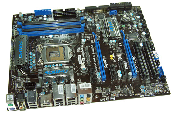
Let’s get to the warts that we found and then discuss a few of the better features that MSI has enabled on this board. We found it perplexing at best that MSI included features for the overclocking audience like the base-clock, power-on, and OC Genie buttons but completely left off features like reset and clear CMOS buttons. The oddly placed JMicron SATA port (seventh port - blue) seems like someone played pin the tail on the donkey for the location when it could have been placed at the top of the board next to the V-Check connector or even as a second eSATA port on the I/O panel. The inclusion of a floppy drive port and even IDE port are also questionable for a board in this category. Otherwise, the layout of this board is just fantastic, especially the PCIe/PCI layout.
The OC Genie overclocking technology could not be easier to use and it works exactly as MSI advertised. Even the 3.3GHz i5/750 and 3.7GHz i7/860 generated overclocks on perfectly acceptable voltages pleased us. We think MSI could have squeezed more out of the i5/750 and improved memory timings a little better, but at least the results made a difference in everyday usage without any fuss. Yet, this feature had a dark side.
It refused to work with several of our test power supplies and we are not talking $35 no name units (they all worked perfectly), but some of the best power supplies from Corsair, BFG, Thermaltake, and others. We could grant a pass on this if it was just one power supply, but we noticed a definite pattern with this board and its big brother, the P55-GD80 when using Channel Well based power supplies.
One area that just drove us crazy at times was overclocking various memory modules. The BIOS features 25 different settings for memory timings and each can be changed on a per-channel basis. Unlike other BIOS releases we have tested, you cannot change the timings of both memory channels with a single entry. Also, under manual mode, there are no auto settings for each memory timing option. So, instead of changing the four basic timings and maybe fine tuning tFAW, tRFC, and B2B only, the user is left with manually setting each sub-timing properly. For a lot of users, this will cause significant additional tuning time to make sure every memory setting is properly set when overclocking. Of course, you will get a crash course on memory tuning so that is a silver lining in the cloud.
Your other choice is to simply leave the memory timings on auto and hope for the best. We say hope for the best because if your SPD is not setup properly with several settings based on memory clock speeds, you could be running your memory at higher than advertised timings or getting stuck in an endless loop when overclocking. We had several modules (1600+ kits) that offered just a couple of memory SPD timings. They were fairly aggressive C6/C7 timings for 1066/1333 clock speeds, yet when we tried to overclock our memory to 2000, these settings were utilized and obviously the board did not POST.
On one hand you can blame the memory suppliers, but these same modules worked perfectly in other boards at high memory clocks. Fine tuning of the BIOS would solve most of these problems, including some tightening up of Vdroop variations that were around 0.05V under load with LLC disabled and an overshoot of 0.03V when enabled. Vdroop follows Intel’s guidelines, but on a enthusiast inspired board like this, it is possible reduce it and not have to enable LLC when overclocking, especially with MSI's excellent hardware design.
The only other two items worth mentioning is that S3 resume worked perfectly up to a 190bclk, after that, this board would not properly resume. We also had a few problems with PCIe speeds above 103 being stable. Both of these will only affect the more adventurous overclockers, but even our sub $100 ASRock P55M Pro had no problems with S3 resume up to a 215 bclk or PCIe speeds up to 110MHz.
Now, that might have sounded like a long list of dirty laundry items but overall this is still an excellent board. MSI's power consumption numbers are first rate and even match or exceed those of boards with less peripherals and slots at idle and near stock conditions. MSI’s continued use of their DrMOS hardware allows for these impressive power consumption numbers and provides for some excellent overclocking results. We also have to hand it to MSI for not playing the “More Phases are better…” game that Gigabyte and ASUS seem to be locked into at this time.
In the end, this board offers a great overclocking experience for users on air or water, especially with an i7/860 as Bclk rates can be kept lower while still hitting current CPU limits and keeping S3 resume enabled. While the board had problems clocking our i5/750 with 8GB of memory above DDR3-2000, running the memory in the DDR3-1680 range at C7 timings offered the same if not better performance as the same memory at DDR3-2055 with C9 timings.
All that said, the MSI P55-GD65 has a great layout, extensive BIOS options, excellent power consumption, and class leading performance in several benchmarks. If the board did not carry a few warts that either could have been solved easily in the design phase or with some additional BIOS tuning, it would certainly be at the top of our list in the mid-range P55 market. So while we were frustrated at times, our overall feeling is that this board deserves your full attention and should be on anyone’s short list when considering a P55 motherboard. Some additional BIOS tuning would make this board award worthy, maybe not in Gold territory, but definitely on the podium.


43 Comments
View All Comments
MadMan007 - Sunday, October 11, 2009 - link
The lack of information regarding PCIe slot assignment when different slots are populated has been SORELY missing from all P55 mobo reviews. It's either laziness or an attempt to cover up shortcomings but it seems pretty important to me - people actually expect to use slots that are present on the board, ya know?I STILL haven't seen an answer to how many lanes the primary graphics slot keeps when the secondary graphics slot is populated with a 1x or 4x card! This affects anyone who has a graphics card and sound card, or TV tuner, or disk controller and given the layout of many boards you're likely going to have to use the secondary graphics slot for those devices.
I am also bothered by the lack of C2Q benchmarks. Loads of people have them and asking whether i5 in particular is a worthwhile upgrade is being ignored.
crab nebula - Tuesday, October 13, 2009 - link
There are two kinds of P55 mbs:1. Non SLI: The PCI Express 2.0 x16 link does not split.
2. SLI x8: The PCI Express 2.0 link splits into two x8 links, usually SLI-certified by NVIDIA
3. SLI x16: The nForce 200 chip is equipped for 2-way SLI: x16, x16 and 3-way SLI: x16, x8, x8.
Most mb of the first type also have a second PCI Express x16 slot which is connected to P55 and works at x4 (1.x in bandwidth).
MSI P55-GD65 is of the second type. If you insert a PCI Express device (of whatever lanes) in the second PCI Express x16 2.0 slot (electrically x8), the first PCI Express x16 2.0 slot also works only at x8.
A problem of P55-GD65 is that the severe (?) limitation of the PCI Express x4 slot is not mentioned in its product page or the manual at all. For example, suppose that a user is using a PCIe x1 sound card in the first PCIe x1 slot and a 2-slot graphics card. If he wants to use a PCIe x1 TV tuner card and insert it in the PCIe x4 slot, then he will suddenly find that his sound card stops working! So he has to use the second PCI Express 2.0 x16 for the TV tuner. Then this decreases the speed of the graphic card to x8!! Although practically this is not a big issue, this limitation still should be mentioned somewhere in the product page or the manual.
"the layout of this board is just fantastic, especially the PCIe/PCI layout." ?? It looks like Gary Key is simply ignorant of this. ASUS and ASRock mbs have much better board layouts in this respect: all expansion slots actually work!
MadMan007 - Tuesday, October 13, 2009 - link
Exactly the type of scenario that no mobo reviews have mentioned and which I was thinking of. Thank you for spelling it out.crab nebula - Tuesday, October 13, 2009 - link
Correction: "There are two kinds of P55 mbs" has to be "There are three kinds of P55 mbs". (The fourth type would be those that use Lucid Hydra 200.)lopri - Sunday, October 11, 2009 - link
I don't know how you don't see PCI Express slot information from the reviews so far? They have been clearly explained or are in the board specification page. There was even a special article regarding P55 chipset PCI Express.MadMan007 - Monday, October 12, 2009 - link
You need to reread and comprehend my post. I'm not asking for specs, obviously those are easy to find, but how lanes get assigned when slots are occupied especially with something other than a graphics card. I guess all reviewers are too lazy to put anything but one or two graphics cards in their test mobos.lopri - Monday, October 12, 2009 - link
I didn't go back and re-read the reviews, but at the time when I read them I was able to tell how the lanes are assigned on a given board. It's not like there are multitude of choices available.. All P55 boards so far (maybe except the one w/ NF200) support either a x16 lane or two x8 lanes from the CPU. Everything else belongs to the PCH and if I remember correctly all reviews made it clear when a physical x16 slot (x4 electrically) belongs to the south bridge.MadMan007 - Monday, October 12, 2009 - link
You still fail to comprehend and say it like I'm a moron who can't read a chipset diagram but your other link at least answered the question about the CPU-based lanes.lopri - Monday, October 12, 2009 - link
http://www.anandtech.com/mb/showdoc.aspx?i=3649">http://www.anandtech.com/mb/showdoc.aspx?i=3649MadMan007 - Monday, October 12, 2009 - link
That is a video card review so no it's not been spelled out in mobo reviews. It's what I figured but hoped the lane splitter chips might be smarter. Thanks for the link though.