NVIDIA's Fermi: Architected for Tesla, 3 Billion Transistors in 2010
by Anand Lal Shimpi on September 30, 2009 12:00 AM EST- Posted in
- GPUs
Architecting Fermi: More Than 2x GT200
NVIDIA keeps referring to Fermi as a brand new architecture, while calling GT200 (and RV870) bigger versions of their predecessors with a few added features. Marginalizing the efforts required to build any multi-billion transistor chip is just silly, to an extent all of these GPUs have been significantly redesigned.
At a high level, Fermi doesn't look much different than a bigger GT200. NVIDIA is committed to its scalar architecture for the foreseeable future. In fact, its one op per clock per core philosophy comes from a basic desire to execute single threaded programs as quickly as possible. Remember, these are compute and graphics chips. NVIDIA sees no benefit in building a 16-wide or 5-wide core as the basis of its architectures, although we may see a bit more flexibility at the core level in the future.
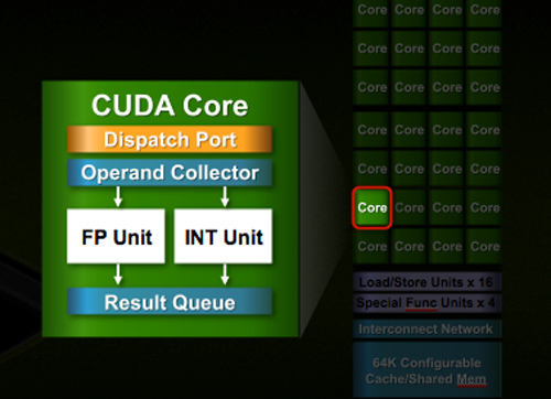
Despite the similarities, large parts of the architecture have evolved. The redesign happened at low as the core level. NVIDIA used to call these SPs (Streaming Processors), now they call them CUDA Cores, I’m going to call them cores.

All of the processing done at the core level is now to IEEE spec. That’s IEEE-754 2008 for floating point math (same as RV870/5870) and full 32-bit for integers. In the past 32-bit integer multiplies had to be emulated, the hardware could only do 24-bit integer muls. That silliness is now gone. Fused Multiply Add is also included. The goal was to avoid doing any cheesy tricks to implement math. Everything should be industry standards compliant and give you the results that you’d expect.
Double precision floating point (FP64) performance is improved tremendously. Peak 64-bit FP execution rate is now 1/2 of 32-bit FP, it used to be 1/8 (AMD's is 1/5). Wow.
NVIDIA isn’t disclosing clock speeds yet, so we don’t know exactly what that rate is yet.
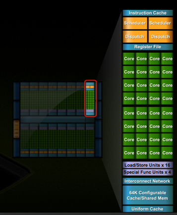
In G80 and GT200 NVIDIA grouped eight cores into what it called an SM. With Fermi, you get 32 cores per SM.

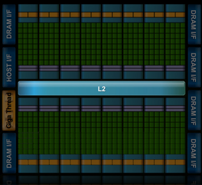
The high end single-GPU Fermi configuration will have 16 SMs. That’s fewer SMs than GT200, but more cores. 512 to be exact. Fermi has more than twice the core count of the GeForce GTX 285.
| Fermi | GT200 | G80 | |
| Cores | 512 | 240 | 128 |
| Memory Interface | 384-bit GDDR5 | 512-bit GDDR3 | 384-bit GDDR3 |
In addition to the cores, each SM has a Special Function Unit (SFU) used for transcendental math and interpolation. In GT200 this SFU had two pipelines, in Fermi it has four. While NVIDIA increased general math horsepower by 4x per SM, SFU resources only doubled.
The infamous missing MUL has been pulled out of the SFU, we shouldn’t have to quote peak single and dual-issue arithmetic rates any longer for NVIDIA GPUs.
NVIDIA organizes these SMs into TPCs, but the exact hierarchy isn’t being disclosed today. With the launch's Tesla focus we also don't know specific on ROPs, texture filtering or anything else related to 3D graphics. Boo.
A Real Cache Hierarchy
Each SM in GT200 had 16KB of shared memory that could be used by all of the cores. This wasn’t a cache, but rather software managed memory. The application would have to knowingly move data in and out of it. The benefit here is predictability, you always know if something is in shared memory because you put it there. The downside is it doesn’t work so well if the application isn’t very predictable.
Branch heavy applications and many of the general purpose compute applications that NVIDIA is going after need a real cache. So with Fermi at 40nm, NVIDIA gave them a real cache.
Attached to each SM is 64KB of configurable memory. It can be partitioned as 16KB/48KB or 48KB/16KB; one partition is shared memory, the other partition is an L1 cache. The 16KB minimum partition means that applications written for GT200 that require 16KB of shared memory will still work just fine on Fermi. If your app prefers shared memory, it gets 3x the space in Fermi. If your application could really benefit from a cache, Fermi now delivers that as well. GT200 did have an L1 texture cache (one per TPC), but the cache was mostly useless when the GPU ran in compute mode.

The entire chip shares a 768KB L2 cache. The result is a reduced penalty for doing an atomic memory op, Fermi is 5 - 20x faster here than GT200.


415 Comments
View All Comments
hazarama - Saturday, October 3, 2009 - link
"Do you see any sign of commercial software support? Anybody Nvidia can point to and say "they are porting $important_app to openCL"? I haven't heard a mention. That pretty much puts Nvidia's GPU computing schemes solely in the realm of academia"Maybe you should check out Snow Leopard ..
samspqr - Friday, October 2, 2009 - link
Well, I do HPC for a living, and I think it's too early to push GPU computing so hard because I've tried to use it, and gave up because it required too much effort (and I didn't know exactly how much I would gain in my particular applications).I've also tried to promote GPU computing among some peers who are even more hardcore HPC users, and they didn't pick it up either.
If even your typical physicist is scared by the complexity of the tool, it's too early.
(as I'm told, there was a time when similar efforts were needed in order to use the mathematical coprocessor...)
Yojimbo - Sunday, October 4, 2009 - link
>>If even your typical physicist is scared by the complexity of the >>tool, it's too early.This sounds good but it's not accurate. Physicists are interested in physics and most are not too keen on learning some new programing technique unless it is obvious that it will make a big difference for them. Even then, adoption is likely to be slow due to inertia. Nvidia is trying to break that inertia by pushing gpu computing. First they need to put the hardware in place and then they need to convince people to use it and put the software in place. They don't expect it to work like a switch. If they think the tools are in place to make it viable, then how is the time to push, because it will ALWAYS require a lot of effort when making the switch.
jessicafae - Saturday, October 3, 2009 - link
Fantastic article.I do bioinformatics / HPC and in our field too we have had several good GPU ports for a handful for algorithms, but nothing so great to drive us to add massive amounts of GPU racks to our clusters. With OpenCL coming available this year, the programming model is dramatically improved and we will see a lot more research and prototypes of code being ported to OpenCL.
I feel we are still in the research phase of GPU computing for HPC (workstations, a few GPU racks, lots of software development work). I am guessing it will be 2+ years till GPU/stream/OpenCL algorithms warrant wide-spread adoption of GPUs in clusters. I think a telling example is the RIKEN 12petaflop supercomputer which is switching to a complete scalar processor approach (100,000 Sparc64 VIIIfx chips with 800,000 cores)
http://www.fujitsu.com/global/news/pr/archives/mon...">http://www.fujitsu.com/global/news/pr/archives/mon...
Thatguy97 - Thursday, May 28, 2015 - link
oh fermi how i miss ya hot underperforming ass