The Real Conroe Successor: Clarkdale & All You Need to Know about Westmere
by Anand Lal Shimpi on September 24, 2009 6:00 PM EST- Posted in
- CPUs
On-package GPU and Graphics Turbo
Arrandale and Clarkdale are two-die packages. There's the 32nm CPU die and next to it is a 45nm DirectX 10 GPU die (no DX11 support until possibly Larrabee).
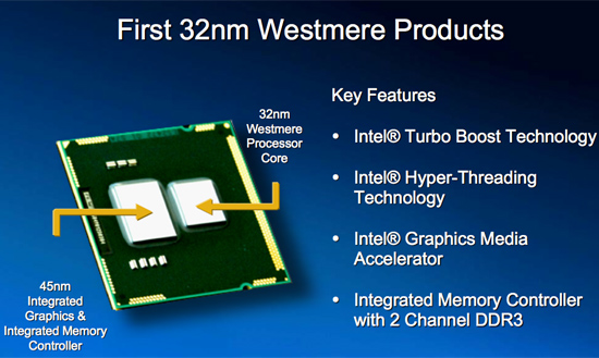
This isn't Larrabee (yet), it's a direct descendent of the graphics in G45. While G45 was built on a 65nm process, the 'dale graphics is built on a 45nm process.
The smaller transistors enable much higher performance. While G45 had 10 shader cores, the 'dale GPU increases that to 12. A number of performance limiting issues have now been resolved, so we should see much more competitive performance from Intel's graphics.
The memory controller has been moved off of the CPU die and is on the GPU die instead. It's still on-package so you get decently low latencies, but it shouldn't technically be as low as on Lynnfield. This is a temporary problem that fixes itself once the CPU/GPU are on the same die with Sandy Bridge.
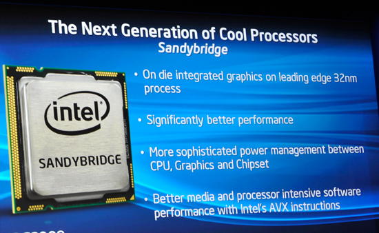
Sandy Bridge brings on-die graphics
I've already explained turbo mode quite a bit so I won't rehash it here. The technology basically allows you to run your CPU at the fastest possible frequency regardless of how many cores are active. Westmere has this.
Arrandale will support graphics turbo modes, while Clarkdale won't. Clarkdale graphics is already running as fast as possible regardless of TDP.
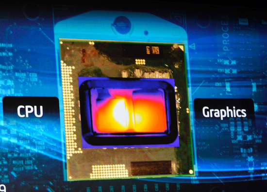
If the GPU demand is higher than the CPU demand, the CPU will allocate more of its TDP to the GPU and vice versa.


96 Comments
View All Comments
jordanclock - Friday, September 25, 2009 - link
I see you're privy to data we are not seeing. Could you please share where you received this information that moving the memory controller to another chip ON THE SAME SOCKET will somehow cause pre-IMC memory latencies? We'd all like to see some actual numbers instead of sensationalist guesses.KaarlisK - Friday, September 25, 2009 - link
I remembered reading about it somewhere.It was from the benchmark here. http://global.hkepc.com/3878/page/5#view">http://global.hkepc.com/3878/page/5#view
Though the latency in this review is higher than Core 2's, which makes it suspect.
As to the why, there are smarter people than me who could answer whether there's any impact from locating the other die on the CPU package or in the chipset.
GeorgeH - Thursday, September 24, 2009 - link
Hopefully more major manufacturers will offer Mini-ITX motherboards this generation. It's nice to see at least one Intel board, but if 775 is any indication it'll be almost ridiculously feature poor.I also hope PS and case manufacturers are paying attention - the current crop of mini-ITX options is pitiful.
Mr Perfect - Saturday, September 26, 2009 - link
Absolutely.I'm impressed that the mITX has what looks to be an x16 PCIe slot on it though. In the past, Intel was always throwing a PCI or x1 slot on them. I think they where afraid that people would stop buying the bigger, more expensive boards. I know I would have.
Hopefully Anand will take a good hard look at this sector.
tomoyo - Friday, September 25, 2009 - link
No kidding! There's a total lack of good mini-itx boards with undervolting features and only one server raid case for mini-itx at all. It's sad because I'm sure a ton of people would love to make a small DIY raid nas system and not deal with the low end parts and lack of OS choice in pre-built nas systems.Aquila76 - Thursday, September 24, 2009 - link
I was going to build an HTPC soon, but if this can really bitstream TrueHD & DTS-MA on a single, low-power chip then I can wait. Next year is going to kill my wallet, but at least I can start saving now!mgl888 - Thursday, September 24, 2009 - link
What's gonna happen after 22nm? 10nm?When are we gonna hit a brick wall and what's Intel plan to do next?
Quantum computing?
Zink - Thursday, September 24, 2009 - link
It looks like there is going to be a big delay after 22nm because the thickness of certain layers in the transistors can not be scaled thinner.Check out 16nm too: http://en.wikipedia.org/wiki/22_nanometer">http://en.wikipedia.org/wiki/22_nanometer
jwilliams4200 - Thursday, September 24, 2009 - link
Each die shrink generation decreases the gate length by a factor of the square root of two (0.707), so that the die area decreases by a factor of two every shrink. To answer your questions, the gate lengths to expect are: 45nm, 32nm, 22nm, 16nm, 11nm, 8nm, 5.6nm ...As to how the lower ones can be achieved, or whether they will be achieved, I will not venture a guess.
CurseTheSky - Thursday, September 24, 2009 - link
Thank you for clarifying that. I always wondered how they determined what the next process size would be. It seemed like they picked arbitrary numbers out of a hat, but now I see that:65 / 2^(1/2) = 45.96
45 / 2^(1/2) = 31.82
32 / 2^(1/2) = 22.63
etc.