The Real Conroe Successor: Clarkdale & All You Need to Know about Westmere
by Anand Lal Shimpi on September 24, 2009 6:00 PM EST- Posted in
- CPUs
Two Cores, Four Threads
Clarkdale is the spiritual successor to Conroe - one of our favorite dual-core processors of all time. It's a dual core chip but with all of the magic of Nehalem. Meaning you get a 64KB L1 per core, 256KB L2 per core but only a 4MB L3 cache. Remember that the L3 cache is shared among all cores and Intel likes to keep the ratio at 2MB per core.
Each core is capable of executing two threads (Hyper Threading). There's of course going to be turbo mode, although the upside shouldn't be too huge on desktop Clarkdale processors.
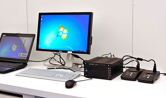
A Clarkdale mini-ITX system
Clarkdale, like the rest of the Nehalem/Westmere family makes extensive use of clock gating. You also get a ~1M transistor PCU that is in charge of keeping power consumption at a minimum. The result is a chip that truly sips power:
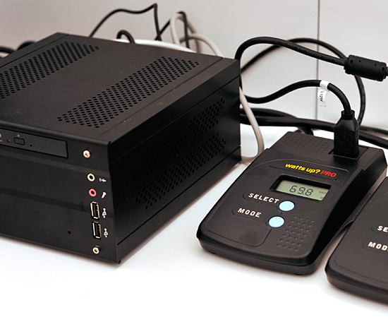
69.8W under Cinebench load
Intel's Clarkdale mini-ITX system used less than 30W at idle and only 70W under load running Cinebench's multi-threaded test. The idle performance is particularly impressive - that's not too far off from an Ion system honestly, but with much better performance.
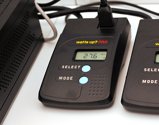
27.6W at idle


96 Comments
View All Comments
jordanclock - Friday, September 25, 2009 - link
I see you're privy to data we are not seeing. Could you please share where you received this information that moving the memory controller to another chip ON THE SAME SOCKET will somehow cause pre-IMC memory latencies? We'd all like to see some actual numbers instead of sensationalist guesses.KaarlisK - Friday, September 25, 2009 - link
I remembered reading about it somewhere.It was from the benchmark here. http://global.hkepc.com/3878/page/5#view">http://global.hkepc.com/3878/page/5#view
Though the latency in this review is higher than Core 2's, which makes it suspect.
As to the why, there are smarter people than me who could answer whether there's any impact from locating the other die on the CPU package or in the chipset.
GeorgeH - Thursday, September 24, 2009 - link
Hopefully more major manufacturers will offer Mini-ITX motherboards this generation. It's nice to see at least one Intel board, but if 775 is any indication it'll be almost ridiculously feature poor.I also hope PS and case manufacturers are paying attention - the current crop of mini-ITX options is pitiful.
Mr Perfect - Saturday, September 26, 2009 - link
Absolutely.I'm impressed that the mITX has what looks to be an x16 PCIe slot on it though. In the past, Intel was always throwing a PCI or x1 slot on them. I think they where afraid that people would stop buying the bigger, more expensive boards. I know I would have.
Hopefully Anand will take a good hard look at this sector.
tomoyo - Friday, September 25, 2009 - link
No kidding! There's a total lack of good mini-itx boards with undervolting features and only one server raid case for mini-itx at all. It's sad because I'm sure a ton of people would love to make a small DIY raid nas system and not deal with the low end parts and lack of OS choice in pre-built nas systems.Aquila76 - Thursday, September 24, 2009 - link
I was going to build an HTPC soon, but if this can really bitstream TrueHD & DTS-MA on a single, low-power chip then I can wait. Next year is going to kill my wallet, but at least I can start saving now!mgl888 - Thursday, September 24, 2009 - link
What's gonna happen after 22nm? 10nm?When are we gonna hit a brick wall and what's Intel plan to do next?
Quantum computing?
Zink - Thursday, September 24, 2009 - link
It looks like there is going to be a big delay after 22nm because the thickness of certain layers in the transistors can not be scaled thinner.Check out 16nm too: http://en.wikipedia.org/wiki/22_nanometer">http://en.wikipedia.org/wiki/22_nanometer
jwilliams4200 - Thursday, September 24, 2009 - link
Each die shrink generation decreases the gate length by a factor of the square root of two (0.707), so that the die area decreases by a factor of two every shrink. To answer your questions, the gate lengths to expect are: 45nm, 32nm, 22nm, 16nm, 11nm, 8nm, 5.6nm ...As to how the lower ones can be achieved, or whether they will be achieved, I will not venture a guess.
CurseTheSky - Thursday, September 24, 2009 - link
Thank you for clarifying that. I always wondered how they determined what the next process size would be. It seemed like they picked arbitrary numbers out of a hat, but now I see that:65 / 2^(1/2) = 45.96
45 / 2^(1/2) = 31.82
32 / 2^(1/2) = 22.63
etc.