AMD's Radeon HD 5870: Bringing About the Next Generation Of GPUs
by Ryan Smith on September 23, 2009 9:00 AM EST- Posted in
- GPUs
More GDDR5 Technologies: Memory Error Detection & Temperature Compensation
As we previously mentioned, for Cypress AMD’s memory controllers have implemented a greater part of the GDDR5 specification. Beyond gaining the ability to use GDDR5’s power saving abilities, AMD has also been working on implementing features to allow their cards to reach higher memory clock speeds. Chief among these is support for GDDR5’s error detection capabilities.
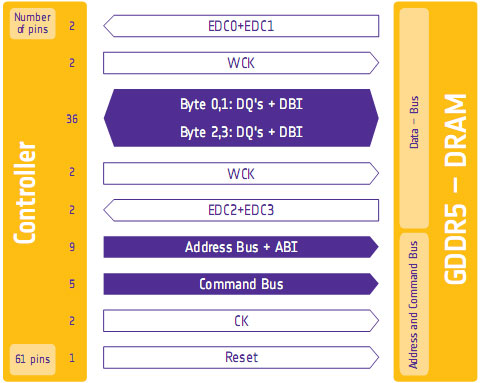
One of the biggest problems in using a high-speed memory device like GDDR5 is that it requires a bus that’s both fast and fairly wide - properties that generally run counter to each other in designing a device bus. A single GDDR5 memory chip on the 5870 needs to connect to a bus that’s 32 bits wide and runs at base speed of 1.2GHz, which requires a bus that can meeting exceedingly precise tolerances. Adding to the challenge is that for a card like the 5870 with a 256-bit total memory bus, eight of these buses will be required, leading to more noise from adjoining buses and less room to work in.
Because of the difficulty in building such a bus, the memory bus has become the weak point for video cards using GDDR5. The GPU’s memory controller can do more and the memory chips themselves can do more, but the bus can’t keep up.
To combat this, GDDR5 memory controllers can perform basic error detection on both reads and writes by implementing a CRC-8 hash function. With this feature enabled, for each 64-bit data burst an 8-bit cyclic redundancy check hash (CRC-8) is transmitted via a set of four dedicated EDC pins. This CRC is then used to check the contents of the data burst, to determine whether any errors were introduced into the data burst during transmission.
The specific CRC function used in GDDR5 can detect 1-bit and 2-bit errors with 100% accuracy, with that accuracy falling with additional erroneous bits. This is due to the fact that the CRC function used can generate collisions, which means that the CRC of an erroneous data burst could match the proper CRC in an unlikely situation. But as the odds decrease for additional errors, the vast majority of errors should be limited to 1-bit and 2-bit errors.
Should an error be found, the GDDR5 controller will request a retransmission of the faulty data burst, and it will keep doing this until the data burst finally goes through correctly. A retransmission request is also used to re-train the GDDR5 link (once again taking advantage of fast link re-training) to correct any potential link problems brought about by changing environmental conditions. Note that this does not involve changing the clock speed of the GDDR5 (i.e. it does not step down in speed); rather it’s merely reinitializing the link. If the errors are due the bus being outright unable to perfectly handle the requested clock speed, errors will continue to happen and be caught. Keep this in mind as it will be important when we get to overclocking.
Finally, we should also note that this error detection scheme is only for detecting bus errors. Errors in the GDDR5 memory modules or errors in the memory controller will not be detected, so it’s still possible to end up with bad data should either of those two devices malfunction. By the same token this is solely a detection scheme, so there are no error correction abilities. The only way to correct a transmission error is to keep trying until the bus gets it right.
Now in spite of the difficulties in building and operating such a high speed bus, error detection is not necessary for its operation. As AMD was quick to point out to us, cards still need to ship defect-free and not produce any errors. Or in other words, the error detection mechanism is a failsafe mechanism rather than a tool specifically to attain higher memory speeds. Memory supplier Qimonda’s own whitepaper on GDDR5 pitches error correction as a necessary precaution due to the increasing amount of code stored in graphics memory, where a failure can lead to a crash rather than just a bad pixel.
In any case, for normal use the ramifications of using GDDR5’s error detection capabilities should be non-existent. In practice, this is going to lead to more stable cards since memory bus errors have been eliminated, but we don’t know to what degree. The full use of the system to retransmit a data burst would itself be a catch-22 after all – it means an error has occurred when it shouldn’t have.
Like the changes to VRM monitoring, the significant ramifications of this will be felt with overclocking. Overclocking attempts that previously would push the bus too hard and lead to errors now will no longer do so, making higher overclocks possible. However this is a bit of an illusion as retransmissions reduce performance. The scenario laid out to us by AMD is that overclockers who have reached the limits of their card’s memory bus will now see the impact of this as a drop in performance due to retransmissions, rather than crashing or graphical corruption. This means assessing an overclock will require monitoring the performance of a card, along with continuing to look for traditional signs as those will still indicate problems in memory chips and the memory controller itself.
Ideally there would be a more absolute and expedient way to check for errors than looking at overall performance, but at this time AMD doesn’t have a way to deliver error notices. Maybe in the future they will?
Wrapping things up, we have previously discussed fast link re-training as a tool to allow AMD to clock down GDDR5 during idle periods, and as part of a failsafe method to be used with error detection. However it also serves as a tool to enable higher memory speeds through its use in temperature compensation.
Once again due to the high speeds of GDDR5, it’s more sensitive to memory chip temperatures than previous memory technologies were. Under normal circumstances this sensitivity would limit memory speeds, as temperature swings would change the performance of the memory chips enough to make it difficult to maintain a stable link with the memory controller. By monitoring the temperature of the chips and re-training the link when there are significant shifts in temperature, higher memory speeds are made possible by preventing link failures.
And while temperature compensation may not sound complex, that doesn’t mean it’s not important. As we have mentioned a few times now, the biggest bottleneck in memory performance is the bus. The memory chips can go faster; it’s the bus that can’t. So anything that can help maintain a link along these fragile buses becomes an important tool in achieving higher memory speeds.


327 Comments
View All Comments
silverblue - Saturday, September 26, 2009 - link
I think you may have been much happier with a 512-bit interface which would result in nearly 2.5x the bandwidth of the 4890, however it remains to be seen whether it'd be a waste or not. Having said that, it could mean for slower GDDR5 thus reducing costs, but wouldn't it be far more problematic to incorporate the wider bus anyway?If ATI throw out such a card with a single GPU on it, a direct comparison with the 5870 (and nVidia's top cards at the time) will be inevitable. The extra bandwidth may be rather under-utilised for anything less than Eyefinity gaming or Crysis at max details ;)
Now all we need is AMD to come back at Intel with a domestic release of its Thuban die (or hurry up with Bulldozer, sheesh) and it'll be a very, very exciting time for people to upgrade.
SiliconDoc - Sunday, September 27, 2009 - link
I want to know how the pinout compares on the 5870 gpu to the 4870/90.Have they doubled the data pins, or is the data jamming in and jamming out, even at 4800mhz ?
Maybe that's why 512bit would help.
Perhaps faster data rate ram, needs also a wider data path, more pins, more paths in and out of the gpu.
I will check the overclock sites that have already posted on this matter.
JarredWalton - Sunday, September 27, 2009 - link
I would assume that the pin count on 5870 isn't radically different from 4870. Granted, we know what assuming can get you, but with the same interface width there's not much reason for it to get substantially more pins. A few changes for power leads to deal with having more transistors, and other minor tweaks are likely, but my bet would be it's within 10% of the pin count of 4870.PorscheRacer - Monday, September 28, 2009 - link
For all those people clamoring on about why ATI didn't go with a 512-bit memory controller I'm going to chime in here with some ATI 512-bit experience. If you're a sharp one reading this, you have already guessed that means I'm going to talk about the R600. Now you can hate the card all you want, but I quite enjoyed this card. First of all, in the R600 it was the last ring-bus. It was a true 512-bit, and large memory controller. I'm not certain on the amount, but I believe it owned about a quarter of the realstate on the die. That's a lot. It also was some of the cause for the chip running hot and why UVD was scrapped from that chip to save room.Now, to keep that 512-bit ring-bus fed, you needed to push large amounts of data to it. The more you increased system bandwidth, the faster the card would be in any task. I've run hundreds of benchmarks over the years and I'm pretty sure Jared and Anand can attest to this. Same goes for overclocking the card. Raising the core didn't do much, but cranking up the VRAM to feed that hungry ring-bus sure did. Prices anyone? I believe $450 and up depending on where you were located. It was on heck of a pricey chip for ATI to make. Enter the die shrunk 3000 series with the 256-bit memory controller and voila. A cheaper chip to make. It never came close to the theoretical performance of the 2900XT, but the 3870 was about 90% of the performance for a lot cheaper. Yeas I know the cores were tweaked and so on in the 3000 series, but they are very similar.
If ATI ever went to a 512-bit bus, which means more PCB layers, higher cost in manufacturing and a larger die, I'd think they'd do it on something like Juniper or wait till 32nm. It's not feasible right now. They technically could go the MCM route with Juniper and get a mashed up version of a 512-bit bus, but I don't think the chips have been designed with that in mind.
Anyways, most computers out there are starved to feed something like the 5870 and higher cards with a 512-bit bus. I just replaced my R600 with an RV740 (hah, went from 80nm to 40nm) and now I don't need to OC the heck out of my bus to keep the card fed. I'm running an old FX-60 setup due to a glowing review on here back in early 2006. Am I the norm? NO, I'm waiting to upgrade. Is the Core i7 9xx the norm? No. You have to build a card to a certain set of people. I'm building my pal a new computer and he's happy with the 5850. The 5870 is overkill for him. It's 80% of the 5870 but a hundred bucks cheaper. Now, I'm sure ATI looked at the 512-bit bus in much the same way. "Wow, that 512-bit bus sure flies, look at those numbers! Oh, it's going to cost us this much die space and more manufacturing costs.... Well, those 256-bit bus numbers are still pretty imperssive and within 80% of the gaming benchmark scores, so we'll go that way"
Or something along those lines....I'm sure that's why nVIDIA's GTX300 is delayed. It's a massive chip, 512-bit bus and so on. Great, they'll take the performance crown again. Will they take my money? If they have something in the $200-$300 range, they have a fighting chance, just like ATI does, or soon to be Intel. Best price for performance will win me over there. I don't care what the bus size is, or how the card could have been better, just as long as I'm happy with the performance for my money. In which case, I'll be here looking forward to a GPU roundoup in the best bang for buck in that price range. Of course it will have DX11, or else there's no point in me upgrading again.
SiliconDoc - Wednesday, September 30, 2009 - link
The GT200 is a 512 bit bus.All the whining and complaining about difficulty means NOTHING.
ati goes the cheapskate sloppy lame route, cooks their cores, has 90C heat, few extra features, and a red raging fanbase filled with repeated tantric lies.
I even posted their own forum here with their 4850 90C+ whines, after some rooster told me his worst fan in the world on his 4850 kept it in the cool 60's like the several Nvidia cards, of course.
The 512bit HD2900 XTX was and is a great card, and even the 256 version still holds it's own. It was well over 500 bucks, was limited production, sold out quickly, and there was HD2900 512bit lesser version that could be flashed to full XTX with a bios upgrade, and it disappeared after it went well over $500.
That HD2900XTX has 115GB bandwidth.
It was REAL competition for the 8800GTX.
--
Of course ati cheaped out on producing any decent quantity, has been losing money, overcharged for it (and got it - but apparently like RUIZ, the "leadership" qualifies for "MORONS!"
---
Now, we'll hear endless crying about expense, about 512bit, and endless crying about core size (nvidia's giant monster), then we'll hear how ati just kicks butt because more dies to a wafer, and they can make a profit, and they can then wipe out nvidia and make them lose money....
BUT JUST THE OPPOSITE HAS BEEN GOING ON FOR SOME NUMBER OF YEARS IN A ROW.
If ati is so pathetic it can't handle making 512bit and selling 512bit, well then , they're PATHETIC.
And, yes, it seems they are PATHETIC.
Someone ought to let ati know there's "competition" and the "competition" pumps out 512bit buses all the time.
I guess when ati "finally catches up to the modern world" they can put out a 512bit again.
In the mean time, they can stick with their cheap pcb with less layers, their cooking hot crammed full electromigration core, and have a bunch of looners that for the very first time in their lives, actually believe that the ghetto is better than Beverly Hills, because they goin fps shootin', man.
Oh, it's so very nice so many gamers have as advice and worry ati's imbalanced sheet and how they can maintain it at a higher level. Such a concern on their minds, a great excuse for why ati cheaps out. I've never seen so many gaming enthusiasts with so much whoring for a company's bottom line. At the same time, nvidia is seen as an evil profit center that throws money around influencing the game production industry. LOL
Yes, it's evil for big green to make money, employ reps, toss millions into game channels, be extremely flexible and pump out 20 differing flavors of cards, so it's not so boring, work so games run well on their product - yes what evil , evil ****rds.
...
Perhaps the little red brokers could cheer some more when they feel ati "has improved it bottom line" by producing a cheap, knocked down, thinner, smaller, hotter, less featured, more negative driver issues, red card, because gamers are so concerned with economics, that they love the billions dollar losers plotted and carried out plans, and hate the company rolling in dollars and helping pump out games and a huge variety of gaming cards...
LOL
Yeah, the last red card that really was worth something, the HD2900512XTX.
That's the other thing that is so funny from these little broker economy whizzes. After they start yakkin about ati's dirt cheap product scheme, it really burns em up that the real cadillac of videocards commands a higher price.
Well, there's a reason a better made, more expensive process, more featured, wider supported in games videocard, is higher priced.
"the great economists" then suddenly turn into raging little angry reds, screeching scalping and unfair and greedy... LOL
Oh it's a hoot.
Zak - Monday, October 5, 2009 - link
I like Nvidia cards too, but if I was a moderator here you'd be banned by now. Relax. Take a pill. No one takes you seriously any more.Z.
SiliconDoc - Saturday, September 26, 2009 - link
The core clock is not doubled, still 850.The memory data rate is not doubled 3600 to 4800.
The bus width is not doubled still 256.
The frame buffer is not doubled, still 1GB
--- From Article Page 1 below ---
" So what’s Cypress in a nutshell? It’s a RV790 (Radeon HD 4890) with virtually everything doubled,.."
---
Ok, so pay attention to the word "virtually".
JarredWalton - Saturday, September 26, 2009 - link
There's no need to double the bus... either double the RAM data rate or double the bus width and you accomplish the same thing. But in a nutshell, everything is doubled relative to HD 4890 except for bandwidth, which only improves by 23%. Similarly, everything is more than double the 4870X2, you don't even need to deal with CrossFire stuff, but the 4870X2 has 50% more total bandwidth.ATI almost certainly isn't completely bandwidth limited with 4890/4870X2, but I think 5870 might just be fast enough that it's running into bandwidth limitations. On the other hand, bandwidth limitations are largely dependent on the game and algorithm. For instance, the Quake/Quake World/Doom games have been extremely bandwidth intensive in the past, and some of the titles Anand tested fall into that category. However, I know of other games that appear to be far less dependent on bandwidth, and the more programmable stuff going on, the more important shader performance becomes.
In the past, Oblivion was a great example of this. NVIDIA's 7800/7900 cards had a lot of bandwidth relative to shader performance, while ATI went the other route. Oblivion was really a strong ATI title (X1800/X1900 series) up until NVIDIA released 8800, which greatly improved NVIDIA's shader performance. Most modern titles tend to be a combination of things.
SiliconDoc - Sunday, September 27, 2009 - link
Note: Edited for ease of response.Well noone makes double the ram data rate, there is NO SUCH DDR5. (No one ever said there was.)
None of it runs at 7200 for videocards.
NVIDIA is using the 512bit bus and 448bit+ on it's top cards, so what is ATI's problem, when that's the only thing available ? (They don't need it enough to increase the cost of the cards to get it.)
Furthermore, the core is still 850, so have the data pins in and out of the core doubled ? I RATHER DOUBT IT. (Obviously it didn't - the specs say it's 256-bit. Did you not read the post?)
So, concievably, we have twice the data to move, on the same core speed, with less than double the DATA PINS in and out. (No, we don't have twice the data to move, unless the 4890 totally maxed out what the RAM could provide. ATI doesn't think this happened, so they only marginally increased bandwidth.)
If the bandwidth is NOT the problem, as you so claim, why then since everything ELSE you say has doubled, the conclusion we have is the ATI core is not up to the task. (If it truly had doubled in every area, and performance didn't double, we'd have a problem. The conclusion sane people will draw is that ATI looked at cost and benefit and decided a 256-bit bus was sufficient for the present. Otherwise they'd need a more complex circuit board, which would increase complexity and cost.)
That's it, it's core tech is so much the same....
LOL
Just love those ATI arguments. (There was no argument, but I'm a troll so I created one!)
When the CORE is overclocked, we will see a framerate increase.
SOOOOO.....
Tell me how the core handles TWICE THE DATA in and out - unless it's pinout count has doubled ? Is ther that much wasted time on the 4890 pins - on the current 5870 pins ? (No one said the core handles twice as much data; theoretically it can, but then deeper buffers would help.)
It may handle double data or nearly internally, but that has to communicate with the ram- etc onboard.
SORRY, once again, not agreeing. (Agreeing with what, that the bandwidth only increased by 23%? Wow, that's amazing. You'd disagree if someone said the sun rises in the east, wouldn't you? Try reading next time before responding instead of arguing for the sake of argument.)
Zool - Sunday, September 27, 2009 - link
The meaning of cache on the gpu is so it doesnt need to read and write to dram memmory too often. The speed of texture cache on 5870 is 1 TB/sec and its sram. And thats just the texture chache. It just shows how much speed is needed to utilize that raw comuting power on the chip. They surely tested the chip with higher speed memory and ended with this bandwith compromis.Also u cant compare the bare peak bandwith. The type of memmory controler and the speed of the GPU(and also cache) should change the real world bandwith like we see with wideferent CPU models and speeds.
When u read xxx GB/s bandwith it doesnt mean it always this fast (they name it peak bandwith always).