AMD's Radeon HD 5870: Bringing About the Next Generation Of GPUs
by Ryan Smith on September 23, 2009 9:00 AM EST- Posted in
- GPUs
Lower Idle Power & Better Overcurrent Protection
One aspect AMD was specifically looking to improve in Cypress over RV770 was idle power usage. The load power usage for RV770 was fine at 160W for the HD4870, but that power usage wasn’t dropping by a great deal when idle – it fell by less than half to 90W. Later BIOS revisions managed to knock a few more watts off of this, but it wasn’t a significant change, and even later designs like RV790 still had limits to their idling abilities by only being able to go down to 60W at idle.
As a consequence, AMD went about designing the Cypress with a much, much lower target in mind. Their goal was to get idle power down to 30W, 1/3rd that of RV770. What they got was even better: they came in past that target by 10%, hitting a final idle power of 27W. As a result the Cypress can idle at 30% of the power as RV770, or as compared to Cypress’s load power of 188W, some 14% of its load power.
Accomplishing this kind of dramatic reduction in idle power usage required several changes. Key among them has been the installation of additional power regulating circuitry on the board, and additional die space on Cypress assigned to power regulation. Notably, all of these changes were accomplished without the use of power-gating to shut down unused portions of the chip, something that’s common on CPUs. Instead all of these changes have been achieved through more exhaustive clock-gating (that is, reducing power consumption by reducing clock speeds), something GPUs have been doing for some time now.
The use of clock-gating is quickly evident when we discuss the idle/2D clock speeds of the 5870, which is 150mhz for the core, and 300mhz for the memory . The idle clock speeds here are significantly lower than the 4870 (550/900), which in the case of the core is the source of its power savings as compared to the 4870. As tweakers who have attempted to manually reduce the idle clocks on RV770 based cards for further power savings have noticed, RV770 actually loses stability in most situations if its core clock drops too low. With the Cypress this has been rectified, enabling it to hit these lower core speeds.
Even bigger however are the enhancements to Cypress’s memory controller, which allow it to utilize a number of power-saving tricks with GDDR5 RAM, along with other features that we’ll get to in a bit. With RV770’s memory controller, it was not capable of taking advantage of very many of GDDR5’s advanced features besides the higher bandwidth abilities. Lacking this full bag of tricks, RV770 and its derivatives were unable to reduce the memory clock speed, which is why the 4870 and other products had such high memory clock speeds even at idle. In turn this limited the reduction in power consumption attained by idling GDDR5 modules.
With Cypress AMD has implemented nearly the entire suite of GDDR5’s power saving features, allowing them to reduce the power usage of the memory controller and the GDDR5 modules themselves. As with the improvements to the core clock, key among the improvement in memory power usage is the ability to go to much lower memory clock speeds, using fast GDDR5 link re-training to quickly switch the memory clock speed and voltage without inducing glitches. AMD is also now using GDDR5’s low power strobe mode, which in turn allows the memory controller to save power by turning off the clock data recovery mechanism. When discussing the matter with AMD, they compared these changes to putting the memory modules and memory controller into a GDDR3-like mode, which is a fair description of how GDDR5 behaves when its high-speed features are not enabled.
Finally, AMD was able to find yet more power savings for Crossfire configurations, and as a result the slave card(s) in a Crossfire configuration can use even less power. The value given to us for an idling slave card is 20W, which is a product of the fact that the slave cards go completely unused when the system is idling. In this state slave cards are still capable of instantaneously ramping up for full-load use, although conceivably AMD could go even lower still by powering down the slave cards entirely at a cost of this ability.
On the opposite side of the ability to achieve such low idle power usage is the need to manage load power usage, which was also overhauled for the Cypress. As a reminder, TDP is not an absolute maximum, rather it’s a maximum based on what’s believed to be the highest reasonable load the card will ever experience. As a result it’s possible in extreme circumstances for the card to need power beyond what its TDP is rated for, which is a problem.
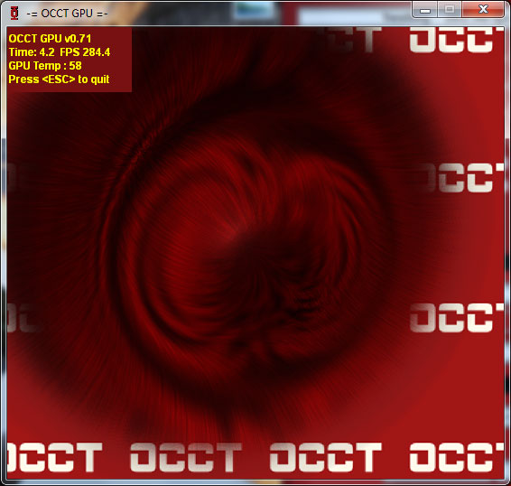
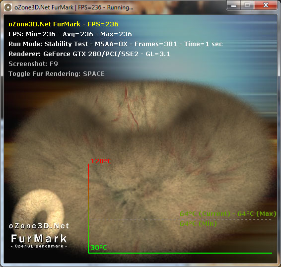
That problem reared its head a lot for the RV770 in particular, with the rise in popularity of stress testing programs like FurMark and OCCT. Although stress testers on the CPU side are nothing new, FurMark and OCCT heralded a new generation of GPU stress testers that were extremely effective in generating a maximum load. Unfortunately for RV770, the maximum possible load and the TDP are pretty far apart, which becomes a problem since the VRMs used in a card only need to be spec’d to meet the TDP of a card plus some safety room. They don’t need to be able to meet whatever the true maximum load of a card can be, as it should never happen.
Why is this? AMD believes that the instruction streams generated by OCCT and FurMark are entirely unrealistic. They try to hit everything at once, and this is something that they don’t believe a game or even a GPGPU application would ever do. For this reason these programs are held in low regard by AMD, and in our discussions with them they referred to them as “power viruses”, a term that’s normally associated with malware. We don’t agree with the terminology, but in our testing we can’t disagree with AMD about the realism of their load – we can’t find anything that generates the same kind of loads as OCCT and FurMark.
Regardless of what AMD wants to call these stress testers, there was a real problem when they were run on RV770. The overcurrent situation they created was too much for the VRMs on many cards, and as a failsafe these cards would shut down to protect the VRMs. At a user level shutting down like this isn’t a very helpful failsafe mode. At a hardware level shutting down like this isn’t enough to protect the VRMs in all situations. Ultimately these programs were capable of permanently damaging RV770 cards, and AMD needed to do something about it. For RV770 they could use the drivers to throttle these programs; until Catalyst 9.8 they detected the program by name, and since 9.8 they detect the ratio of texture to ALU instructions (Ed: We’re told NVIDIA throttles similarly, but we don’t have a good control for testing this statement). This keeps RV770 safe, but it wasn’t good enough. It’s a hardware problem, the solution needs to be in hardware, particularly if anyone really did write a power virus in the future that the drivers couldn’t stop, in an attempt to break cards on a wide scale.
This brings us to Cypress. For Cypress, AMD has implemented a hardware solution to the VRM problem, by dedicating a very small portion of Cypress’s die to a monitoring chip. In this case the job of the monitor is to continually monitor the VRMs for dangerous conditions. Should the VRMs end up in a critical state, the monitor will immediately throttle back the card by one PowerPlay level. The card will continue operating at this level until the VRMs are back to safe levels, at which point the monitor will allow the card to go back to the requested performance level. In the case of a stressful program, this can continue to go back and forth as the VRMs permit.
By implementing this at the hardware level, Cypress cards are fully protected against all possible overcurrent situations, so that it’s not possible for any program (OCCT, FurMark, or otherwise) to damage the hardware by generating too high of a load. This also means that the protections at the driver level are not needed, and we’ve confirmed with AMD that the 5870 is allowed to run to the point where it maxes out or where overcurrent protection kicks in.
On that note, because card manufacturers can use different VRMs, it’s very likely that we’re going to see some separation in performance on FurMark and OCCT based on the quality of the VRMs. The cheapest cards with the cheapest VRMs will need to throttle the most, while luxury cards with better VRMs would need to throttle little, if at all. This should make little difference in stock performance on real games and applications (since as we covered earlier, we can’t find anything that pushes a card to excess) but it will likely make itself apparent in overclocking. Overclocked cards - particularly those with voltage modifications – may hit throttle situations in normal applications, which means the VRMs will make a difference here. It also means that overclockers need to keep an eye on clock speeds, as the card shutting down is no longer a tell-tale sign that you’re pushing it too hard.
Finally, while we’re discussing the monitoring chip, we may as well talk about the rest of its features. Along with monitoring the GPU, it also is a PWM controller. This means that the PWM controller is no longer a separate part that card builders add themselves, and as such we won’t be seeing any cards using a 2pin fixed speed fan to save money on the PWM controller. All Cypress cards (and presumably, all derivatives) will have the ability to use a 4pin fan built-in.


327 Comments
View All Comments
silverblue - Saturday, September 26, 2009 - link
I think you may have been much happier with a 512-bit interface which would result in nearly 2.5x the bandwidth of the 4890, however it remains to be seen whether it'd be a waste or not. Having said that, it could mean for slower GDDR5 thus reducing costs, but wouldn't it be far more problematic to incorporate the wider bus anyway?If ATI throw out such a card with a single GPU on it, a direct comparison with the 5870 (and nVidia's top cards at the time) will be inevitable. The extra bandwidth may be rather under-utilised for anything less than Eyefinity gaming or Crysis at max details ;)
Now all we need is AMD to come back at Intel with a domestic release of its Thuban die (or hurry up with Bulldozer, sheesh) and it'll be a very, very exciting time for people to upgrade.
SiliconDoc - Sunday, September 27, 2009 - link
I want to know how the pinout compares on the 5870 gpu to the 4870/90.Have they doubled the data pins, or is the data jamming in and jamming out, even at 4800mhz ?
Maybe that's why 512bit would help.
Perhaps faster data rate ram, needs also a wider data path, more pins, more paths in and out of the gpu.
I will check the overclock sites that have already posted on this matter.
JarredWalton - Sunday, September 27, 2009 - link
I would assume that the pin count on 5870 isn't radically different from 4870. Granted, we know what assuming can get you, but with the same interface width there's not much reason for it to get substantially more pins. A few changes for power leads to deal with having more transistors, and other minor tweaks are likely, but my bet would be it's within 10% of the pin count of 4870.PorscheRacer - Monday, September 28, 2009 - link
For all those people clamoring on about why ATI didn't go with a 512-bit memory controller I'm going to chime in here with some ATI 512-bit experience. If you're a sharp one reading this, you have already guessed that means I'm going to talk about the R600. Now you can hate the card all you want, but I quite enjoyed this card. First of all, in the R600 it was the last ring-bus. It was a true 512-bit, and large memory controller. I'm not certain on the amount, but I believe it owned about a quarter of the realstate on the die. That's a lot. It also was some of the cause for the chip running hot and why UVD was scrapped from that chip to save room.Now, to keep that 512-bit ring-bus fed, you needed to push large amounts of data to it. The more you increased system bandwidth, the faster the card would be in any task. I've run hundreds of benchmarks over the years and I'm pretty sure Jared and Anand can attest to this. Same goes for overclocking the card. Raising the core didn't do much, but cranking up the VRAM to feed that hungry ring-bus sure did. Prices anyone? I believe $450 and up depending on where you were located. It was on heck of a pricey chip for ATI to make. Enter the die shrunk 3000 series with the 256-bit memory controller and voila. A cheaper chip to make. It never came close to the theoretical performance of the 2900XT, but the 3870 was about 90% of the performance for a lot cheaper. Yeas I know the cores were tweaked and so on in the 3000 series, but they are very similar.
If ATI ever went to a 512-bit bus, which means more PCB layers, higher cost in manufacturing and a larger die, I'd think they'd do it on something like Juniper or wait till 32nm. It's not feasible right now. They technically could go the MCM route with Juniper and get a mashed up version of a 512-bit bus, but I don't think the chips have been designed with that in mind.
Anyways, most computers out there are starved to feed something like the 5870 and higher cards with a 512-bit bus. I just replaced my R600 with an RV740 (hah, went from 80nm to 40nm) and now I don't need to OC the heck out of my bus to keep the card fed. I'm running an old FX-60 setup due to a glowing review on here back in early 2006. Am I the norm? NO, I'm waiting to upgrade. Is the Core i7 9xx the norm? No. You have to build a card to a certain set of people. I'm building my pal a new computer and he's happy with the 5850. The 5870 is overkill for him. It's 80% of the 5870 but a hundred bucks cheaper. Now, I'm sure ATI looked at the 512-bit bus in much the same way. "Wow, that 512-bit bus sure flies, look at those numbers! Oh, it's going to cost us this much die space and more manufacturing costs.... Well, those 256-bit bus numbers are still pretty imperssive and within 80% of the gaming benchmark scores, so we'll go that way"
Or something along those lines....I'm sure that's why nVIDIA's GTX300 is delayed. It's a massive chip, 512-bit bus and so on. Great, they'll take the performance crown again. Will they take my money? If they have something in the $200-$300 range, they have a fighting chance, just like ATI does, or soon to be Intel. Best price for performance will win me over there. I don't care what the bus size is, or how the card could have been better, just as long as I'm happy with the performance for my money. In which case, I'll be here looking forward to a GPU roundoup in the best bang for buck in that price range. Of course it will have DX11, or else there's no point in me upgrading again.
SiliconDoc - Wednesday, September 30, 2009 - link
The GT200 is a 512 bit bus.All the whining and complaining about difficulty means NOTHING.
ati goes the cheapskate sloppy lame route, cooks their cores, has 90C heat, few extra features, and a red raging fanbase filled with repeated tantric lies.
I even posted their own forum here with their 4850 90C+ whines, after some rooster told me his worst fan in the world on his 4850 kept it in the cool 60's like the several Nvidia cards, of course.
The 512bit HD2900 XTX was and is a great card, and even the 256 version still holds it's own. It was well over 500 bucks, was limited production, sold out quickly, and there was HD2900 512bit lesser version that could be flashed to full XTX with a bios upgrade, and it disappeared after it went well over $500.
That HD2900XTX has 115GB bandwidth.
It was REAL competition for the 8800GTX.
--
Of course ati cheaped out on producing any decent quantity, has been losing money, overcharged for it (and got it - but apparently like RUIZ, the "leadership" qualifies for "MORONS!"
---
Now, we'll hear endless crying about expense, about 512bit, and endless crying about core size (nvidia's giant monster), then we'll hear how ati just kicks butt because more dies to a wafer, and they can make a profit, and they can then wipe out nvidia and make them lose money....
BUT JUST THE OPPOSITE HAS BEEN GOING ON FOR SOME NUMBER OF YEARS IN A ROW.
If ati is so pathetic it can't handle making 512bit and selling 512bit, well then , they're PATHETIC.
And, yes, it seems they are PATHETIC.
Someone ought to let ati know there's "competition" and the "competition" pumps out 512bit buses all the time.
I guess when ati "finally catches up to the modern world" they can put out a 512bit again.
In the mean time, they can stick with their cheap pcb with less layers, their cooking hot crammed full electromigration core, and have a bunch of looners that for the very first time in their lives, actually believe that the ghetto is better than Beverly Hills, because they goin fps shootin', man.
Oh, it's so very nice so many gamers have as advice and worry ati's imbalanced sheet and how they can maintain it at a higher level. Such a concern on their minds, a great excuse for why ati cheaps out. I've never seen so many gaming enthusiasts with so much whoring for a company's bottom line. At the same time, nvidia is seen as an evil profit center that throws money around influencing the game production industry. LOL
Yes, it's evil for big green to make money, employ reps, toss millions into game channels, be extremely flexible and pump out 20 differing flavors of cards, so it's not so boring, work so games run well on their product - yes what evil , evil ****rds.
...
Perhaps the little red brokers could cheer some more when they feel ati "has improved it bottom line" by producing a cheap, knocked down, thinner, smaller, hotter, less featured, more negative driver issues, red card, because gamers are so concerned with economics, that they love the billions dollar losers plotted and carried out plans, and hate the company rolling in dollars and helping pump out games and a huge variety of gaming cards...
LOL
Yeah, the last red card that really was worth something, the HD2900512XTX.
That's the other thing that is so funny from these little broker economy whizzes. After they start yakkin about ati's dirt cheap product scheme, it really burns em up that the real cadillac of videocards commands a higher price.
Well, there's a reason a better made, more expensive process, more featured, wider supported in games videocard, is higher priced.
"the great economists" then suddenly turn into raging little angry reds, screeching scalping and unfair and greedy... LOL
Oh it's a hoot.
Zak - Monday, October 5, 2009 - link
I like Nvidia cards too, but if I was a moderator here you'd be banned by now. Relax. Take a pill. No one takes you seriously any more.Z.
SiliconDoc - Saturday, September 26, 2009 - link
The core clock is not doubled, still 850.The memory data rate is not doubled 3600 to 4800.
The bus width is not doubled still 256.
The frame buffer is not doubled, still 1GB
--- From Article Page 1 below ---
" So what’s Cypress in a nutshell? It’s a RV790 (Radeon HD 4890) with virtually everything doubled,.."
---
Ok, so pay attention to the word "virtually".
JarredWalton - Saturday, September 26, 2009 - link
There's no need to double the bus... either double the RAM data rate or double the bus width and you accomplish the same thing. But in a nutshell, everything is doubled relative to HD 4890 except for bandwidth, which only improves by 23%. Similarly, everything is more than double the 4870X2, you don't even need to deal with CrossFire stuff, but the 4870X2 has 50% more total bandwidth.ATI almost certainly isn't completely bandwidth limited with 4890/4870X2, but I think 5870 might just be fast enough that it's running into bandwidth limitations. On the other hand, bandwidth limitations are largely dependent on the game and algorithm. For instance, the Quake/Quake World/Doom games have been extremely bandwidth intensive in the past, and some of the titles Anand tested fall into that category. However, I know of other games that appear to be far less dependent on bandwidth, and the more programmable stuff going on, the more important shader performance becomes.
In the past, Oblivion was a great example of this. NVIDIA's 7800/7900 cards had a lot of bandwidth relative to shader performance, while ATI went the other route. Oblivion was really a strong ATI title (X1800/X1900 series) up until NVIDIA released 8800, which greatly improved NVIDIA's shader performance. Most modern titles tend to be a combination of things.
SiliconDoc - Sunday, September 27, 2009 - link
Note: Edited for ease of response.Well noone makes double the ram data rate, there is NO SUCH DDR5. (No one ever said there was.)
None of it runs at 7200 for videocards.
NVIDIA is using the 512bit bus and 448bit+ on it's top cards, so what is ATI's problem, when that's the only thing available ? (They don't need it enough to increase the cost of the cards to get it.)
Furthermore, the core is still 850, so have the data pins in and out of the core doubled ? I RATHER DOUBT IT. (Obviously it didn't - the specs say it's 256-bit. Did you not read the post?)
So, concievably, we have twice the data to move, on the same core speed, with less than double the DATA PINS in and out. (No, we don't have twice the data to move, unless the 4890 totally maxed out what the RAM could provide. ATI doesn't think this happened, so they only marginally increased bandwidth.)
If the bandwidth is NOT the problem, as you so claim, why then since everything ELSE you say has doubled, the conclusion we have is the ATI core is not up to the task. (If it truly had doubled in every area, and performance didn't double, we'd have a problem. The conclusion sane people will draw is that ATI looked at cost and benefit and decided a 256-bit bus was sufficient for the present. Otherwise they'd need a more complex circuit board, which would increase complexity and cost.)
That's it, it's core tech is so much the same....
LOL
Just love those ATI arguments. (There was no argument, but I'm a troll so I created one!)
When the CORE is overclocked, we will see a framerate increase.
SOOOOO.....
Tell me how the core handles TWICE THE DATA in and out - unless it's pinout count has doubled ? Is ther that much wasted time on the 4890 pins - on the current 5870 pins ? (No one said the core handles twice as much data; theoretically it can, but then deeper buffers would help.)
It may handle double data or nearly internally, but that has to communicate with the ram- etc onboard.
SORRY, once again, not agreeing. (Agreeing with what, that the bandwidth only increased by 23%? Wow, that's amazing. You'd disagree if someone said the sun rises in the east, wouldn't you? Try reading next time before responding instead of arguing for the sake of argument.)
Zool - Sunday, September 27, 2009 - link
The meaning of cache on the gpu is so it doesnt need to read and write to dram memmory too often. The speed of texture cache on 5870 is 1 TB/sec and its sram. And thats just the texture chache. It just shows how much speed is needed to utilize that raw comuting power on the chip. They surely tested the chip with higher speed memory and ended with this bandwith compromis.Also u cant compare the bare peak bandwith. The type of memmory controler and the speed of the GPU(and also cache) should change the real world bandwith like we see with wideferent CPU models and speeds.
When u read xxx GB/s bandwith it doesnt mean it always this fast (they name it peak bandwith always).