ATI Radeon HD 4890 vs. NVIDIA GeForce GTX 275
by Anand Lal Shimpi & Derek Wilson on April 2, 2009 12:00 AM EST- Posted in
- GPUs
The Cards and The Test
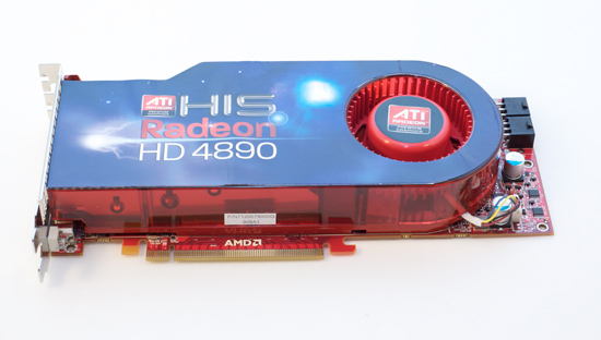
In the AMD department, we received two cards. One was an overclocked part from HIS and the other was a stock clocked part from ASUS. Guess which one AMD sent us for the review. No, it's no problem, we're used to it. This is what happens when we get cards from NVIDIA all the time. They argue and argue for the inclusion of overclocked numbers in GPU reviews when it's their GPU we're looking at. Of course when the tables are turned so are the opinions. We sincerely appreciate ASUS sending us this card and we used it for our tests in this article. The original intent of trying to get a hold of two cards was to run CrossFire numbers, but we only have one GTX 275 and we would prefer to wait until we can compare the two to get into that angle.
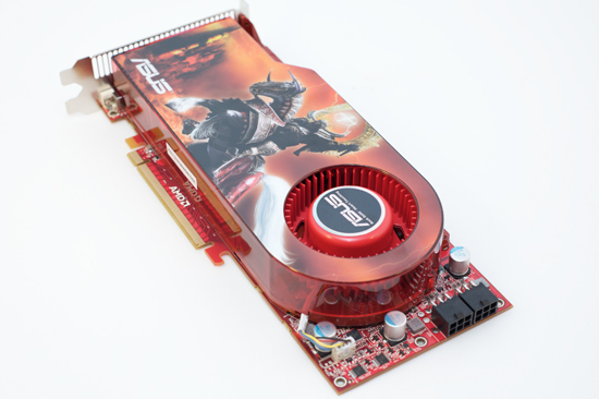
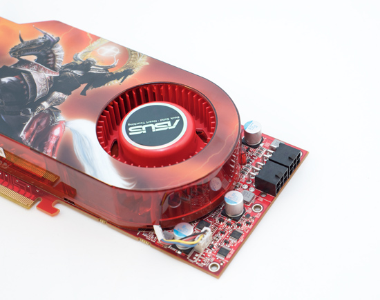
The ASUS card also includes a utility called Voltage Tweaker that allows gamers to increase some voltages on their hardware to help improve overclocking. We didn't have the chance to play with the feature ourselves, but more control is always a nice feature to have.
For the Radeon HD 4890 our hardware specs are pretty simple. Take a 4870 1GB and overclock it. Crank the core up 100 MHz to 850 MHz and the memory clock up 75 MHz to 975 MHz. That's the Radeon HD 4890 in a nutshell. However, to reach these clock levels, AMD revised the core by adding decoupling capacitors, new timing algorithms, and altered the ASIC power distribution for enhanced operation. These slight changes increased the transistor count from 956M to 959M. Otherwise, the core features/specifications (texture units, ROPs, z/stencil) remain the same as the HD4850/HD4870 series.
Most vendors will also be selling overclocked variants that run the core at 900 MHz. AMD would like to treat these overclocked parts like they are a separate entity altogether. But we will continue to treat these parts as enhancements of the stock version whether they come from NVIDIA or AMD. In our eyes, the difference between, say, an XFX GTX 275 and an XFX GTX 275 XXX is XFX's call; the latter is their part enhancing the stock version. We aren't going to look at the XFX 4890 and the XFX 4890 XXX any differently. In doing reviews of vendor's cards, we'll consider overclocked performance closely, but for a GPU launch, we will be focusing on the baseline version of the card.
On the NVIDIA side, we received a reference version of the GTX 275. It looks similar to the design of the other GT200 based hardware.
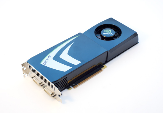
Under the hood here is the same setup as half of a GTX 295 but with higher clock speeds. That means that the GTX 275 has the memory amount and bandwidth of the GTX 260 (448-bit wide bus), but the shader count of the GTX 280 (240 SPs). On top of that, the GTX 275 posts clock speeds closer to the GTX 285 than the GTX 280. Core clock is up 31 MHz from a GTX 280 to 633 MHz, shader clock is up 108 MHz to 1404 MHz, and memory clock is also up 108 MHz to 2322. Which means that in shader limited cases we should see performance closer to the GTX 285 and in bandwicth limited cases we'll still be faster than the GTX 216 because of the clock speed boost across the board.
Rather than just an overclock of a pre-existing card, this is a blending of two configurations combined with an overclock from the two configurations from which it was born. And sure, it's also half a GTX 295, and that is convenient for NVIDIA. It's not just that it's different, it's that this setup should have a lot to offer especially in games that aren't bandwidth limited.
That wraps it up for the cards we're focusing on today. Here's our test system, which is the same as for our GTS 250 article except for the addition of a couple drivers.
The Test
| Test Setup | |
| CPU | Intel Core i7-965 3.2GHz |
| Motherboard | ASUS Rampage II Extreme X58 |
| Video Cards | ATI Radeon HD 4890 ATI Radeon HD 4870 1GB ATI Radeon HD 4870 512MB ATI Radeon HD 4850 NVIDIA GeForce GTX 285 NVIDIA GeForce GTX 280 NVIDIA GeForce GTX 275 NVIDIA GeForce GTX 260 core 216 |
| Video Drivers | Catalyst 8.12 hotfix, 9.4 Beta for HD 4890 ForceWare 185.65 |
| Hard Drive | Intel X25-M 80GB SSD |
| RAM | 6 x 1GB DDR3-1066 7-7-7-20 |
| Operating System | Windows Vista Ultimate 64-bit SP1 |
| PSU | PC Power & Cooling Turbo Cool 1200W |


294 Comments
View All Comments
lk7900 - Monday, April 27, 2009 - link
Can you please die? Prefearbly by getting crushed to death, or by getting your face cut to shreds with a
pocketknife.
I hope that you get curb-stomped, f ucking retard
Shut the *beep* up f aggot, before you get your face bashed in and cut
to ribbons, and your throat slit.
http://www.youtube.com/watch?v=QGt3lpxyo1U">http://www.youtube.com/watch?v=QGt3lpxyo1U
I wish you a truly painful, bloody, gory, and agonizing death, *beep*
Veteran - Thursday, April 2, 2009 - link
BTW. 4890 is not a rebadge or something, it is an improved core (check xbitlabs), it has 3M more pixels and about 22 sqmm more diesizeVeteran - Thursday, April 2, 2009 - link
pixels should be transistors offcourse.....GamerBad - Thursday, August 5, 2010 - link
I am not sure what all the conversation here is about.I will tell you a bit my graphics card.
First,
I am an GeForce man through and through. I will tell you why.
I have never purchased a GeForce card that was faulty. Luck?
My current computer is running all Asus. Twin Ati Radeon 4890's ...
and so far.. I am on my third replacement graphics card. The first one had memory problems. Second was doa... third.. well.. this one overheats and crashes.
The Radeon may be better than the GeForce when it works. I really dont notice a difference.
So to me.. it is quality of craftsmanship that makes the difference.
Currently I am very unhappy with Radeon becuase I build my new system for this graphics setup. My Asus mother board dosent support dual GeForce only Radeon.
It seems I am stuck sending my graphics cards back and praying eventually I will get one that is not a lemon.