Intel's 32nm Update: The Follow-on to Core i7 and More
by Anand Lal Shimpi on February 11, 2009 12:00 AM EST- Posted in
- CPUs
The Manufacturing Roadmap
The tick-tock cadence may have come about at the microprocessor level, but its roots have always been in manufacturing. As long as I’ve been running AnandTech, Intel has introduced a new manufacturing process every two years. In fact, since 1989 Intel has kept up this two year cycle.
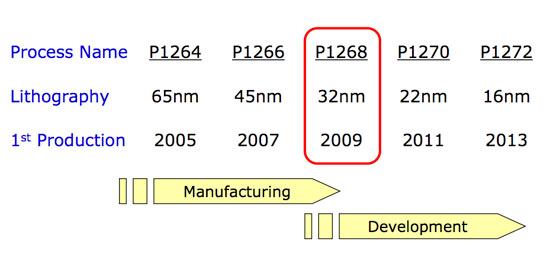
We saw the first 45nm CPUs with the Penryn core back in late 2007. Penryn, released at the very high end, spent most of 2008 making its way mainstream. Now you can buy a 45nm Penryn CPU for less than $100.
The next process technology, which Intel refers to internally as P1268, shrinks transistor feature size down to 32nm. The table above shows you that first production will be in 2009 and, after a brief pause to check your calendars, that means this year. More specifically, Q4 of this year.
I’ll get to the products in a moment, but first let’s talk about the manufacturing process itself.
Here we have our basic CMOS transistor:
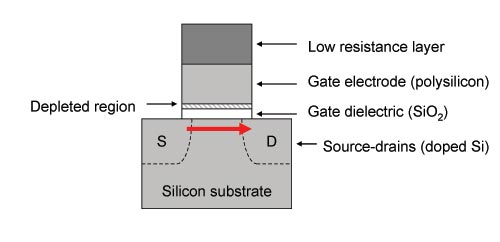
Current flows from source to drain when the transistor is on, and it isn’t supposed to flow when it’s off. Now as you shrink the transistor, all of its parts shrink. At 65nm Intel found that it couldn’t shrink the gate dielectric any more without leaking too much current through the gate itself. Back then the gate dielectric was 1.2nm thick (about the thickness of 5 atoms), but at 45nm Intel’s switched from a SiO2 gate dielectric to a high-k one using Hafnium. That’s where the high-k comes from.
The gate electrode also got replaced at 45nm with a metal to help increase drive current (more current flows when you want it to). That’s where the metal gate comes from.
The combination of the two changes to the basic transistor gave us Intel’s high-k + metal gate transistors at 45nm, and at 32nm we have the second generation of those improvements.
The high-k gate dielectric gets a little thinner (equivalent to a 0.9nm SiO2 gate, but presumably thicker since it’s Hafnium based, down from 1.0nm at 45nm ) and we’ve still got a metal gate.
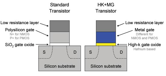
At 32nm the transistors are approximately 70% the size of Intel’s 45nm hk + mg transistors, allowing Intel to pack more in a smaller area.
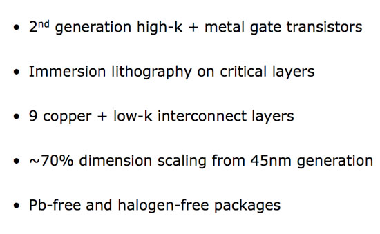
The big change here is that Intel is using immersion lithography on critical metal layers in order to continue to use existing 193nm lithography equipment. The smaller your transistors are, the higher resolution your equipment has to be in order to actually build them. Immersion lithography is used to increase the resolution of existing lithography equipment without requiring new technologies. It is a costlier approach, but one that becomes necessary as you scale below 45nm. Note that AMD to made the switch to immersion lithography at 45nm.
![]()
Intel reported significant gains in transistor performance at 32nm; the graphs below help explain:
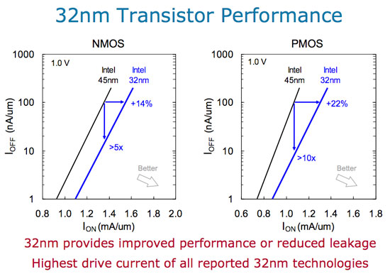
We’re looking at the comparison of leakage current vs. drive current for both 32nm NMOS and PMOS transistors. The new transistors showcase a huge improvement in power efficiency. You can either run them faster or run them at the same speed and significantly reduce leakage current by a magnitude of greater than 5 - 10x compared to Intel’s 45nm transistors. Intel claims that its 32nm transistors boast the highest drive current of all reported 32nm technologies at this point, which admittedly there aren’t many.
The power/performance characteristics of Intel’s 32nm process make it particularly attractive for mobile applications. But more on that later.


64 Comments
View All Comments
blyndy - Wednesday, February 11, 2009 - link
Let me see if I've got this straight: in 2H'09 (I would actually bet Q3'09) we will finally see the Core i5 quads-cores (Lynnfield/Clarksfield) (on a new LGA-1156 socket), which should have been released in Dec'08.So the 45nm Core i5 quads will be the highest performing CPU available for LGA-1156, positioning above the 32nm Clarkdale/Arrandale dual-cores (the 'Core i5 Duo' maybe?) which arrive in Q4'09
How do they indent to make the LGA-1366 platform have better overclockability, i7 and i5 are almost the same, are they going to actively prevent OC'ing on i5? that would be ridiculous.
Somehow I don't think that the artificial socket segmentation will have a significant number of enthusiast herded into LGA-1366 to get the higher margin cash-cow that Intel has planned it to be.
Triple Omega - Sunday, February 15, 2009 - link
Intel isn't going to artificially limit overclocking directly, but it is indirectly by redirecting the better chips to 1366. So the i7 CPU's will be cherry-picked versions of the i5's and thus will overclock better. Besides that the only socket with Extreme versions will be 1366.(Though that is a niche within a niche really)philosofool - Wednesday, February 11, 2009 - link
Overclockers are a very small fraction of the market. I'm not even sure intel is thinking about overclockability when they engineer chips. Overclockability is more an artefact of good engineering than a design goal from the outset. Overclockers are always paranoid that intel or AMD is out to get them by intentionally crippling chips. There just aren't enough of us for Intel to be concerned. We're like 1% of the total CPU market.Pretty much every chip that intel has released at any price point since the introduction of Core 2 has been wonderfully overclockable. I wouldn't worry that Intel is going to change that soon, especially since Core i5 is basically just mainstream processor with the same design fundamentals as the excellent i7.
JonnyDough - Wednesday, February 11, 2009 - link
Although I understand it's a hobby, I don't care if people can overclock or not. As long as we have fast chips at a good price and they're faster than what we have...I mean, why would you care? Isn't it all about SPEED?ssj4Gogeta - Wednesday, February 11, 2009 - link
i5 probably won't have an extreme version.Bezado11 - Wednesday, February 11, 2009 - link
I wouldn't be surprised if the opposite was true. I'm really sick of all the hype on shrinking creates less heat. Look at the gpu industry, ever since they started shrinking things got hotter and hotter, and now it seems with i7 even though it's not a die shrink and we are use to 45nm by now, the new hardware to support minor changes in architecture of the cpu seem to make things run hotter.I7 is way to hot. The newest GPU's run way to hot.
Lightnix - Thursday, February 12, 2009 - link
But you're making an unfair comparison - for example, the current latest GPUs have only been produced on the newest nodes, ever. Now, if we take for example, a Radeon 3870 vs. a Radeon 2900 XT, the former draws far less power and will overclock better on air, almost directly as a result of them shrinking from a 80nm to a 55nm process, despite them performing exactly the same. Another example is the Core 2 E8000 series and E6000 series. Despite the increase in cache size, the E8000 dissipates little enough heat that they can provide them with a very tiny heatsink compared to the earlier 65nm cores, and objectively they draw much less power at the same clock speed because they run at lower volts.You can see this sort of thing again and again throughout the technology industry, Coppermine (180nm) -> Tualatin(130nm), GeForce 7800 -> 7900, G80 -> G92, etc., etc.
If you were to compare say, a GTX280 to a 8800 GTX and say the former draws much more power than the 8800 GTX, AND it's produced on a smaller process - well, yes, but that's because they've clocked it higher and there are far more transistors (twice as many, in fact).
Mr Perfect - Thursday, February 12, 2009 - link
That's because every time they shrink the chips they pack in new features and push the clock speed to the bleeding edge. If all they did was die shrink the old tech, we'd all be running something like an Atom CPU right now. Atoms closely resemble Pentium 3s, but on modern manufacturing only draw what? 5 watts?V3ctorPT - Wednesday, February 11, 2009 - link
The GPU's run hotter, because they pack double the transistors with a new shrink, than their previous HW... Reduction of the manufacturing process enables that we can have so much more transistors in the same place, of course it gets hot...JonnyDough - Wednesday, February 11, 2009 - link
I think you need to re-read the manufacturing roadmap page. It details the leakage gain (heat).