The RV770 Story: Documenting ATI's Road to Success
by Anand Lal Shimpi on December 2, 2008 12:00 AM EST- Posted in
- GPUs
Re-evaluating Strategy, Creating the RV770 in 2005
Remembering what lead to success rather than the success itself is generally more important, and around 2005 ATI had another R300 moment. What made R300 successful was ATI re-evaluating the way it made GPUs and deciding on something that made sense. At the time, it made sense for ATI to work towards building the biggest chip possible, win at the high end and translate that into better, more competitive products at all other price points. It is worth mentioning that part of R300’s continued success was due to the fact that NVIDIA slipped up royally with the GeForce FX, it was the perfect storm and ATI capitalized. ATI built the biggest chip and NVIDIA had no real answer for some time to come.
Just as Intel bumped into the power wall when it tried to ramp Pentium 4 clock speeds to ridiculous levels, ATI was noticing that GPUs were getting a little too big for comfort. Design cycles were getting longer, die size was growing and financially there were some things that didn’t quite make sense when it came to making these large GPUs.
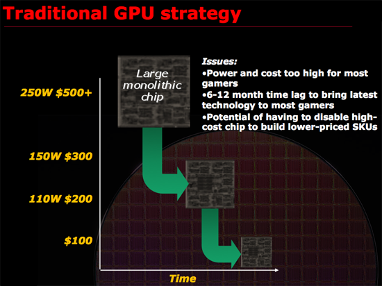
ATI asserted that a very large GPU, without the use of repair structures or harvesting (two techniques I’ll describe in a bit) may only have a 30% yield. That means for every 100 GPUs produced on a single wafer, only 30% of them would be fully functional and could be sold as advertised. Manufacturing these complex circuits is particularly expensive, those fab plants easily cost a couple of billion dollars to build and thus having most of your wafer go to waste isn’t really a good way of running a business.
Thankfully there are ways to improve that crappy 30% yield to a value north of 90%. The first is a technique generally known as repairability. The idea behind repairability is simple: build redundancy into your design. If you have a unit with 10 shader processors, actually build 11 but use one as a spare should there be a defect in any of the remaining processors. The same technique is often used for on-die memory, include additional cells so that a defect in one part of a cache won’t render the entire chip unusable. There are tradeoffs here however, if you build in too much repairability then you run the risk of having a die that’s large but offers no additional performance benefit. If you don’t build in enough repairability then your yield suffers.
Harvesting is another technique that all of you are quite familiar with, although its street name is feature binning. The idea here is that you assume that only a small percentage of the die on a wafer will be completely functional, but instead of throwing away the ones that aren’t fully functional, you disable features and sell them as a lower end part. For example, if your target architecture has 10 shader processors but only 30% of your production will have 10 working shader processors but 50% of the production will have 8 working units you’d sell a model with 10 SPs and a model with 8 SPs, the latter being at a reduced cost. This way instead of throwing away 70% of the wafer, you only throw away 20% - and if possible you could make a third SKU with fewer number of functional SPs and use close to 100% of the wafer.
Yields do improve over time, and what eventually happens if you build a product relying on harvesting is you hurt yourself financially. In the example above where you have two configurations of the same die, yields will eventually improve to the point where your 8 SP die could just as easily have 10 functional SPs but you have to sell them as reduced functionality parts because you’ve built up market demand for them. In a sense, you’re selling something worth $1 for $0.80. You could always create a new version of the chip with a smaller die, but that takes additional engineering resources, time and money.
The most recent public example of die harvesting was actually with NVIDIA’s GT200. The GeForce GTX 260 was simply a harvested version of the GTX 280 with 192 SPs vs. 240. As yields improved, NVIDIA introduced the GeForce GTX 260 Core 216 with 216 SPs. Note that NVIDIA didn’t use any repairability for the shader processors on GT200 there are no more than 240 functional SPs on a GT200 die, but that’s because NVIDIA would rely on harvesting anyway - if any of the 240 SPs didn’t work the chip would be branded as a GTX 260 or Core 216.
This is in stark contrast to RV770 where both versions of the GPU were functionally identical, the only differences were clock speeds and power requirements. But from a die standpoint, ATI didn’t have to sell any reduced versions of the chip to keep yields high.
Note that whether or not a company has to rely on harvesting doesn’t really impact the end user. In this case, the GeForce GTX 260 Core 216 actually benefitted the end user as it manages to deliver the same sort of value that AMD does with the Radeon HD 4870. It isn’t ideal for NVIDIA financially and if a company has to rely on harvesting for too long it will eventually take its toll, but I suspect that in the GT200 case NVIDIA will bail itself out with a 55nm revision of GT200 before things get too bad.
ATI didn’t want to build a GPU that would rely on excessive repair and harvesting to keep yields high. And then came the killer argument: building such a GPU was no longer in the best interests of its customers.
Sidenote: Building a GPU
Before we get too far down the rabbit hole it’s worth adding some perspective. ATI’s RV770 design took three years of work, that means ATI started in 2005. It takes about a year for manufacturability from tapeout to final product ship, another 1 - 1.5 years for design and another year for architecture.
The team that I met with in Santa Clara was talking about designs that would be out in 2012, we’re talking 4 TFLOPS of performance here, 4x the speed of RV770.
Decisions being made today are going to impact those products and in a sense it’s a big guessing game, ATI has no idea what NVIDIA will have in 2012 and NVIDIA has no idea what ATI will have. Each company simply tries to do the best it can for the customers and hopes they’ve got the right mix of performance, price and power.
To give you an idea of the intensity of some of these debates, Carrell debated, every evening, for three hours, for three weeks, the amount of repairability that would go into the RV770. Building redundant structures in the RV770 was an even bigger deal than before because ATI was going to be working within serious die constraints, simply making the chip bigger wasn’t an option. Repair structures in the RV770 wouldn’t add any performance but would increase the die size, on an already large chip that’s fine, but on a chip that’s supposed to target the sweet spot and can’t grow without limit it’s a big deal.


116 Comments
View All Comments
Spivonious - Wednesday, December 3, 2008 - link
I totally agree! Articles like this one are what separates Anandtech from the multitude of other tech websites.goinginstyle - Wednesday, December 3, 2008 - link
I have to admit this is one of the best articles I have read anywhere on the web in a long time. It is very insightful, interesting, and even compelling at times. Can you do a follow up, only from an NVIDIA perspective.Jorgisven - Wednesday, December 3, 2008 - link
I totally agree. This article is superbly written. One of the best tech articles I've read in a long long time, out of any source, magazine or online. I highly doubt nVidia will be as willing to expose their faults as easily as ATI was to expose their success; but I could be entirely mistaken on that.In either case, well done Anand. And well done ATI! Snagged the HD4850 two days after release during the 25% off Visiontek blunder from Best Buy during release week. I've been happy with it since and can still kick around the 8800GT performance like yesterday's news.
JonnyDough - Wednesday, December 3, 2008 - link
I agree about the insight especially. Gave us a real look at the decision making behind the chips.This got me excited about graphics again, and it leaves me eager to see what will happen in the coming years. This kind of article is what will draw readers back. Thank you Anandtech and the red team for this amazing back stage pass.
magreen - Wednesday, December 3, 2008 - link
Great article! Really compelling story, too.Thanks AMD/ATI for making this possible!
And thanks Anand for continually being the best on the web.
JPForums - Wednesday, December 3, 2008 - link
Like others have said, this is probably the best article I've read in recent memory. It was IMHO well written and interesting. Kudos to ATI as well for divulging the information.I second the notion that similar articles from nVidia and Intel would also be interesting. Any chance of AMD's CPU division doing something similar? I always find the architectural articles interesting, but they gain more significance when you understand the reasoning behind the design.
jordanclock - Wednesday, December 3, 2008 - link
This is easily one of my favorite articles on this website. It really puts a lot of aspects of the GPU design process into perspective, such as the shear amount of time it takes to design one.I also think this article really adds a great deal of humanity to GPU design. The designers of these marvels of technology are often forgotten (if ever known by most) and to hear the story of one of the most successful architectures to date, from the people that fought for this radical departure... It's amazing, to say the least.
I really envy you, Anand. You get to meet the geek world's superheroes.
pattycake0147 - Wednesday, December 3, 2008 - link
I couldn't agree more! This could be the best article I've read here at anandtech period. The performance reviews are great, but once in a while you need something different or refreshing and this is just precisely that.LordanSS - Wednesday, December 3, 2008 - link
Yep, I agree with that. This is simply one of the best articles I've read here.Awesome work, Anand.
Clauzii - Wednesday, December 3, 2008 - link
I totally agree.