The RV770 Story: Documenting ATI's Road to Success
by Anand Lal Shimpi on December 2, 2008 12:00 AM EST- Posted in
- GPUs
Re-evaluating Strategy, Creating the RV770 in 2005
Remembering what lead to success rather than the success itself is generally more important, and around 2005 ATI had another R300 moment. What made R300 successful was ATI re-evaluating the way it made GPUs and deciding on something that made sense. At the time, it made sense for ATI to work towards building the biggest chip possible, win at the high end and translate that into better, more competitive products at all other price points. It is worth mentioning that part of R300’s continued success was due to the fact that NVIDIA slipped up royally with the GeForce FX, it was the perfect storm and ATI capitalized. ATI built the biggest chip and NVIDIA had no real answer for some time to come.
Just as Intel bumped into the power wall when it tried to ramp Pentium 4 clock speeds to ridiculous levels, ATI was noticing that GPUs were getting a little too big for comfort. Design cycles were getting longer, die size was growing and financially there were some things that didn’t quite make sense when it came to making these large GPUs.
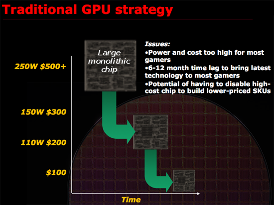
ATI asserted that a very large GPU, without the use of repair structures or harvesting (two techniques I’ll describe in a bit) may only have a 30% yield. That means for every 100 GPUs produced on a single wafer, only 30% of them would be fully functional and could be sold as advertised. Manufacturing these complex circuits is particularly expensive, those fab plants easily cost a couple of billion dollars to build and thus having most of your wafer go to waste isn’t really a good way of running a business.
Thankfully there are ways to improve that crappy 30% yield to a value north of 90%. The first is a technique generally known as repairability. The idea behind repairability is simple: build redundancy into your design. If you have a unit with 10 shader processors, actually build 11 but use one as a spare should there be a defect in any of the remaining processors. The same technique is often used for on-die memory, include additional cells so that a defect in one part of a cache won’t render the entire chip unusable. There are tradeoffs here however, if you build in too much repairability then you run the risk of having a die that’s large but offers no additional performance benefit. If you don’t build in enough repairability then your yield suffers.
Harvesting is another technique that all of you are quite familiar with, although its street name is feature binning. The idea here is that you assume that only a small percentage of the die on a wafer will be completely functional, but instead of throwing away the ones that aren’t fully functional, you disable features and sell them as a lower end part. For example, if your target architecture has 10 shader processors but only 30% of your production will have 10 working shader processors but 50% of the production will have 8 working units you’d sell a model with 10 SPs and a model with 8 SPs, the latter being at a reduced cost. This way instead of throwing away 70% of the wafer, you only throw away 20% - and if possible you could make a third SKU with fewer number of functional SPs and use close to 100% of the wafer.
Yields do improve over time, and what eventually happens if you build a product relying on harvesting is you hurt yourself financially. In the example above where you have two configurations of the same die, yields will eventually improve to the point where your 8 SP die could just as easily have 10 functional SPs but you have to sell them as reduced functionality parts because you’ve built up market demand for them. In a sense, you’re selling something worth $1 for $0.80. You could always create a new version of the chip with a smaller die, but that takes additional engineering resources, time and money.
The most recent public example of die harvesting was actually with NVIDIA’s GT200. The GeForce GTX 260 was simply a harvested version of the GTX 280 with 192 SPs vs. 240. As yields improved, NVIDIA introduced the GeForce GTX 260 Core 216 with 216 SPs. Note that NVIDIA didn’t use any repairability for the shader processors on GT200 there are no more than 240 functional SPs on a GT200 die, but that’s because NVIDIA would rely on harvesting anyway - if any of the 240 SPs didn’t work the chip would be branded as a GTX 260 or Core 216.
This is in stark contrast to RV770 where both versions of the GPU were functionally identical, the only differences were clock speeds and power requirements. But from a die standpoint, ATI didn’t have to sell any reduced versions of the chip to keep yields high.
Note that whether or not a company has to rely on harvesting doesn’t really impact the end user. In this case, the GeForce GTX 260 Core 216 actually benefitted the end user as it manages to deliver the same sort of value that AMD does with the Radeon HD 4870. It isn’t ideal for NVIDIA financially and if a company has to rely on harvesting for too long it will eventually take its toll, but I suspect that in the GT200 case NVIDIA will bail itself out with a 55nm revision of GT200 before things get too bad.
ATI didn’t want to build a GPU that would rely on excessive repair and harvesting to keep yields high. And then came the killer argument: building such a GPU was no longer in the best interests of its customers.
Sidenote: Building a GPU
Before we get too far down the rabbit hole it’s worth adding some perspective. ATI’s RV770 design took three years of work, that means ATI started in 2005. It takes about a year for manufacturability from tapeout to final product ship, another 1 - 1.5 years for design and another year for architecture.
The team that I met with in Santa Clara was talking about designs that would be out in 2012, we’re talking 4 TFLOPS of performance here, 4x the speed of RV770.
Decisions being made today are going to impact those products and in a sense it’s a big guessing game, ATI has no idea what NVIDIA will have in 2012 and NVIDIA has no idea what ATI will have. Each company simply tries to do the best it can for the customers and hopes they’ve got the right mix of performance, price and power.
To give you an idea of the intensity of some of these debates, Carrell debated, every evening, for three hours, for three weeks, the amount of repairability that would go into the RV770. Building redundant structures in the RV770 was an even bigger deal than before because ATI was going to be working within serious die constraints, simply making the chip bigger wasn’t an option. Repair structures in the RV770 wouldn’t add any performance but would increase the die size, on an already large chip that’s fine, but on a chip that’s supposed to target the sweet spot and can’t grow without limit it’s a big deal.


116 Comments
View All Comments
Sahrin - Monday, January 25, 2010 - link
Anand,I love this piece. Not sure if you'll get notified, but while doing some research on the performance of Hybrid Crossfire, I came back - it was interesting to see the tone of the piece, and hear about the guys at ATI talking vageuly about what would become the 5870. Fascinating stuff, I've got to put a bookmark in my calendar to remind me to come back to this next year when RV970 is released (pending no further difficulties).
Any chance of a follow-up piece with the guys in SC?
caldran - Wednesday, December 24, 2008 - link
the gpu industry is squeezing more and more transistors(SP s or what ever) .it would be energy efficient if it could disable some cores when there is less load than reducing clock frequency and 2D mode.just like in the latest AMD processor.a HD 4350 would consume power less than HD 4850 in IDLE right.bupkus - Wednesday, December 10, 2008 - link
I couldn't put it down until I had finished.Extremely enjoyable write!
yacoub - Tuesday, December 9, 2008 - link
"that R580 would be similar in vain"You want vein. Not vain, not vane. Vein. =)
CEO Ballmer - Sunday, December 7, 2008 - link
You people don't mention their alliance with MS!http://fakesteveballmer.blogspot.com">http://fakesteveballmer.blogspot.com
BoFox - Sunday, December 7, 2008 - link
LOL!!!!!BoFox - Sunday, December 7, 2008 - link
Great article--a nice read!However...
From how I remember history:
In 2006, when the legendary X1900XTX took the world by surprise, actually beating the scarce and coveted 7800GTX-512, I bought it. It was king of the hill from January 2006 until the 7950GX2 stole the crown back for the fastest "single-slot" solution about 6 months later around June 2006, only a few months after the smaller 90nm 7900GTX was *finally* released in April 2006. Everybody started hailing Nvidia again although it was really an SLI dual-gpu solution sandwiched into one PCI-E slot. Perhaps it was the quad-gpu thingy that sounded so cool. It was obviously over-hyped but really took the attention away from ATI.
GDDR4 on the X1950XTX hardly did any good, since it was a bit late (Sept 2006) with only like 3-4 performance increase over the X1900. Well then the 8800GTX came in Nov 2006 and had a similar impact that the 9700Pro had.
As everybody wanted to see how the R600 would do, it was delayed, and disappointed hugely in June 2007. The 8800GTX/Ultra kept on selling for around $600 for nearly 12 months straight, making history. 80nm just did not cut it for the R600, so ATI wanted to have its dual-GPU single card REVENGE against Nvidia. And it would be even better this time since it's done on a single PCB, not a sandwiched solution like Nvidia's 7900GX2. Hence the tiny RV770 chips made on unexpected 55nm process! The 3870X2 did beat the 8800GTX in most reviews, but had to use Crossfire just like with SLI. Also, the 3870X2 only used GDDR3, unlike the single 3870 with fast GDDR4.
But Nvidia still took the attention away from the 3870 series by tossing an 8800GT up for grabs. When the 3870X2 came out in Jan 2008, Nvidia touted its upcoming 9800GX2 (to be released one month afterwards). So, Nvidia stopped ATI with an ace up its sleeve.
Round 2 for ATI's revenge: The 4870X2. And it worked this time! There was no way that Nvidia could expect the 4870 to be *that much* better than the 3870. Everybody was saying the 4870 would be 50% faster, and Nvidia yawned at that, thinking that the 4870 still couldnt touch the 9800GTX or 9800GX2 when crossfired. Plus Nvidia expected the 4870 to still have the "AA bug" since the 3870 did not fix it from the 2900XT, and the 4870 had a similar architecture. Boy, Nvidia was all wrong there! The 4870 actually ended up being *50%* faster than the 9800GTX in some games.
So, now ATI has earned its vengeance with its single-slot dual-GPU solution that Nvidia had with its 7900GX2 and 9800GX2 a while ago. With the 4870X2 destroying the GTX 280, ATI does indeed have its crown or "halo".
Unfortunately, Quad-crossfire hardly does well against the GTX 280 in SLI. We now know that quad-GPU solutions give a far lower "bang-per-GPU" due to poor driver optimizations, etc.. So most enthusiast gamers with the money and a 2560x1600 monitor are running two GTX 280's right now instead of two 4870X2's.. oh well!
One thing not mentioned about GDDR5 is that it eats power like mad! The memory alone consumes 40W, even at idle, and that is one of the reasons why the 4870 does not idle so well. If ATI reduces the speed low enough, it messes up the Aero graphics in Vista. It would have been nice if ATI released an intermediate 4860 version with GDDR4 memory at 2800+MHz effective.
Now, I cannot even start to expect what the RV870 will be like. I think Nvidia is going to really want its own revenge this time around, being so financially hurt with the whole 9800 - GTX 200 range plus being unable to release a 55nm version of G200 to this day. Nvidia just cannot beat the 4870X2 with a dual G200 on 55nm, and this is the reason for the re-spins (delays) with an attempt to reduce the power consumption while maintaining the necessary clock speed. Pardon me for pointing out the obvious...
Hope my mini-article was a nice supplement to the main article! :)
CarrellK - Sunday, December 7, 2008 - link
Not bad at all.BTW, 55nm has less to do with how good the RV770 is than the re-architecture & re-design our engineers did post-RV670.
To illustrate, scale the RV770 from 55nm to 65nm (only core scales, not pads & analog) and see how big it is. Now compare that to anything else in 65nm.
Pretty darned good engineers I'd say.
BoFox - Sunday, December 7, 2008 - link
True, and nowhere in the article was it pointed out that since the AA algorithm relied on the shaders, simply upping the shader units from 320 to a whopping 800 completely solved the weak AA performance that plagued 2900's and 3870's. It did not cost too much chip die size or power consumption either. ATI certainly did design the R600 with the future in mind (by moving AA to the shader units, with future expansion). Now the 4870 does amazing well with 8x FSAA, even beating the GTX 280 in some games.I wanted to edit my above post by saying that the dual G200 needed to have low enough power consumption so that it could still be cooled effectively in a single-slot sandwich cooling solution. The 4870X2 has a dual-slot cooler, but Nvidia just cannot engineer the G200 on a single PCB with the architecture that they are currently using (monster chip die size, and 16 memory chips that scales with 448-bit to 512-bit bandwidth instead of using 8 memory chips with 512-bit bandwidth). That is why Nvidia must make the move to GDDR5 memory, or else re-design the memory architecture to a greater degree. Just my thoughts... I still have no idea what we'll be seeing in 2009!
papapapapapapapababy - Saturday, December 6, 2008 - link
more like uber mega retards, right? if they are so smart... why do they keep making such terrible, horrible, shitty drivers?why?
i really really, really want to buy a 4850, i really do. but im not going to do it. im going to go and buy the 9800gt. And i know is just a re branded 8800gt. And i know nvidia is making shitty @ explosive hardware ( my 8600gt just died) And i know that gpu is slower, older, oced 65nm tech. And that nvidia is pushing gimmicky tricks " physics" and buying devs. but guess what? NVIDIA = good, clean drivers. New game? New drivers there. Fast. UN-Bloated drivers, that work, is is that hard ati? Really. or maybe you guys just suck?
Im going to pick all tech@ because of that. Thats how much i fkn hate your bloated and retarded drivers ATI. Install ms, framework for a broken control panel? stupid. And whats up with all those unnecessary services eating my memory and cpu cycles? ATI Hotkey poller?, ATI Smart?, ATI2EVXX.exe, ATI2EVXX.exe,NET 2.0 ? always there and the damm thing takes forever to load? Nvidia dsnt use any bloated crap, so why do you feel entitled to polute my pc with your bloated drivers?
AGAIN HORRIBLE DRIVERS ATI! I DONT WANT A SINGLE EXTRA SERVICE! i just build a pc for a friend. I choose the hd4670, beautiful card, really cool, fast, efficient. I love it. I want one for myself. But the drivers? ARg, i ended up using just the display driver and still the memory consumption was utterly retarded compared to my nvidia card.
so geniuses? move your asses and fix your drivers.
thanks, and good job with your hard.