The Dark Knight: Intel's Core i7
by Anand Lal Shimpi & Gary Key on November 3, 2008 12:00 AM EST- Posted in
- CPUs
Nehalem.
Nuh - hay - lem
At least that's how Intel PR pronounces it.
I've been racking my brain for the past month on how best to review this thing, what angle to take, it's tough. You see, with Conroe the approach was simple: the Pentium 4 was terrible, AMD proudly wore its crown and Intel came in and turned everyone's world upside down. With Nehalem, the world is fine, it doesn't need fixing. AMD's pricing is quite competitive, Intel's performance is solid, power consumption isn't getting out of control...things are nice.
But we've got that pesky tick-tock cadence and things have to change for the sake of change (or more accurately, technological advancement, I swear I'm not getting cynical in my old age):
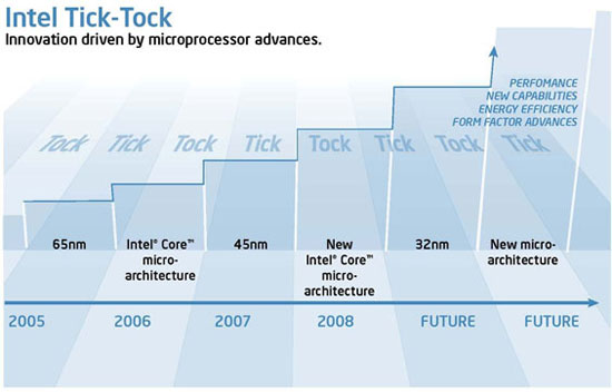
2008, that's us, that's Nehalem.
Could Nehalem ever be good enough? It's the first tock after Conroe, that's like going on stage after the late Richard Pryor, it's not an enviable position to be in. Inevitably Nehalem won't have the same impact that Conroe did, but what could Intel possibly bring to the table that it hasn't already?
Let's go ahead and get started, this is going to be interesting...
Nehalem's Architecture - A Recap
I spent 15 pages and thousands of words explaining Intel's Nehalem architecture in detail already, but what I'm going to try and do now is summarize that in a page. If you want greater detail please consult the original article, but here are the cliff's notes.
Nehalem
Nehalem, as I've mentioned countless times before, is a "tock" processor in Intel's tick-tock cadence. That means it's a new microarchitecture but based on an existing manufacturing process, in this case 45nm.
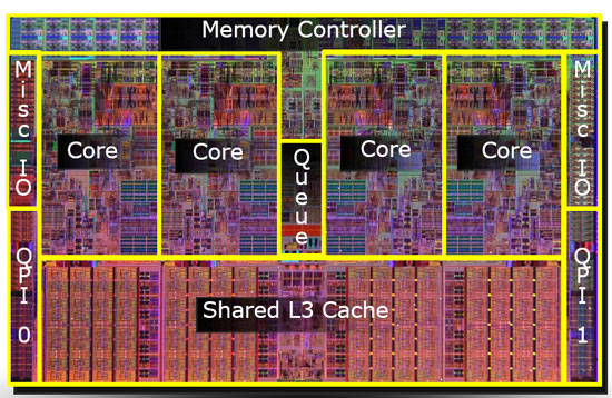
A quad-core Nehalem is made up of 731M transistors, down from 820M in Yorkfield, the current quad-core Core 2s based on the Penryn microarchitecture. The die size has gone up however, from 214 mm^2 to 263 mm^2. That's fewer transistors but less densely packed ones, part of this is due to a reduction in cache size and part of it is due to a fundamental rearchitecting of the microprocessor.
Nehalem is Intel's first "native" quad-core design, meaning that all four cores are a part of one large, monolithic die. Each core has its own L1 and L2 caches, and all four sit behind a large 8MB L3 cache. The L1 cache remains unchanged from Penryn (the current 45nm Core 2 architecture), although it is slower at 4 cycles vs. 3. The L2 cache gets a little faster but also gets a lot smaller at 256KB per core, whereas the lowest end Penryns split 3MB of L2 among two cores. The L3 cache is a new addition and serves as a common pool that all four cores can access, which will really help in cache intensive multithreaded applications (such as those you'd encounter in a server). Nehalem also gets a three-channel, on-die DDR3 memory controller, if you haven't heard by now.
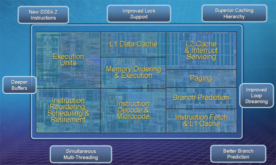
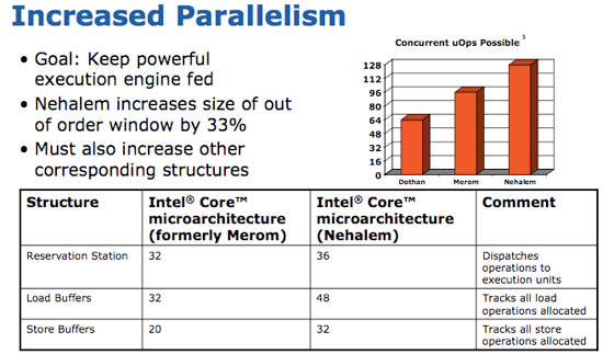
At the core level, everything gets deeper in Nehalem. The CPU is just as wide as before and the pipeline stages haven't changed, but the reservation station, load and store buffers and OoO scheduling window all got bigger. Peak execution power hasn't gone up, but Nehalem should be much more efficient at using its resources than any Core microarchitecture before it.
Once again to address the server space Nehalem increases the size of its TLBs and adds a new 2nd level unified TLB. Branch prediction is also improved, but primarily for database applications.
Hyper Threading is back in its typical 2-way fashion, so a single quad-core Nehalem can work on 8 threads at once. Here we have yet another example of Nehalem making more efficient use of the execution resources rather than simply throwing more transistors at the problem. With Penryn Intel hit nearly 1 billion transistors for a desktop quad-core chip, clearly Nehalem was an attempt to both address the server market and make more efficient use of those transistors before the next big jump and crossing the billion transistor mark.


73 Comments
View All Comments
Kaleid - Monday, November 3, 2008 - link
http://www.guru3d.com/news/intel-core-i7-multigpu-...">http://www.guru3d.com/news/intel-core-i...and-cros...bill3 - Monday, November 3, 2008 - link
Umm, seems the guru3d gains are probably explained by them using a dual core core2dou versus quad core i7...Quad core's run multi-gpu quiet a bit better I believe.tynopik - Monday, November 3, 2008 - link
what about those multi-threading tests you used to run with 20 tabs open in firefox while running av scan while compressing some files while converting something else while etc etc?this might be more important for daily performance than the standard desktop benchmarks
D3SI - Monday, November 3, 2008 - link
So the low end i7s are OC'able?
what the hell is toms hardware talking about lol
conquerist - Monday, November 3, 2008 - link
Concerning x264, Nehalem-specific improvements are coming as soon as the developers are free from their NDA.See http://x264dev.multimedia.cx/?p=40">http://x264dev.multimedia.cx/?p=40.
Spectator - Monday, November 3, 2008 - link
can they do some CUDA optimizations?. im guessing that video hardware has more processors than quad core intel :PIf all this i7 is new news and does stuff xx faster with 4 core's. how does 100+ core video hardware compare?.
Yes im messing but giant Intel want $1k for best i7 cpu. when likes of nvid make bigger transistor count silicon using a lesser process and others manufacture rest of vid card for $400-500 ?
Where is the Value for money in that. Chukkle.
gramboh - Monday, November 3, 2008 - link
The x264 team has specifically said they will not be working on CUDA development as it is too time intensive to basically start over from scratch in a more complex development environment.npp - Monday, November 3, 2008 - link
CUDA Optimizations? I bet you don't understand completely what you're talking about. You can't just optimize a piece of software for CUDA, you MUST write it from scratch for CUDA. That's the reason why you don't see too much software for nVidia GPUs, even though the CUDA concept was introduced at least two years ago. You have the BadaBOOM stuff, but it's far for mature, and the reason is that writing a sensible application for CUDA isn't exactly an easy task. Take your time to look at how it works and you'll understand why.You can't compare the 100+ cores of your typical GPU with a quad core directly, they are fundamentaly different in nature, with your GPU "cores" being rather limited in functionality. GPGPU is a nice hype, but you simply can't offload everything on a GPU.
As a side note, top-notch hardware always carries price premium, and Intel has had this tradition with high-end CPUs for quite a while now. There are plenty of people who need absolutely the fastest harware around and won't hesitate paying it.
Spectator - Monday, November 3, 2008 - link
Some of us want more info.A) How does the integrated Thermal sensor work with -50+c temps.
B) Can you Circumvent the 130W max load sensor
C) what are all those connection points on the top of the processor for?.
lol. Where do i put the 2B pencil to. to join that sht up so i dont have to worry about multiply settings or temp sensors or wattage sensors.
Hey dont shoot the messenger. but those top side chip contacts seem very curious and obviously must serve a purpose :P
Spectator - Monday, November 3, 2008 - link
Wait NO. i have thought about it..The contacts on top side could be for programming the chips default settings.
You know it makes sence.Perhaps its adjustable sram style, rather than burning connections.
yes some technical peeps can look at that. but still I want the fame for suggesting it first. lmao.
Have fun. but that does seem logical to build in some scope for alteration. alot easier to manufacture 1 solid item then mod your stock to suit market when you feel its neccessary.
Spectator.