NVIDIA GeForce GTX 260 Core 216: Competition for the 4870
by Anand Lal Shimpi & Derek Wilson on September 16, 2008 12:00 AM EST- Posted in
- GPUs
Nearly a year ago I wrote about something I called "sensible naming" with respect to GPUs. It was at the time of the Radeon HD 3800 series launch where AMD unveiled a much cleaner, simpler way of naming its cards. Gone were the suffixes (for the most part) and instead what we were left with was this:
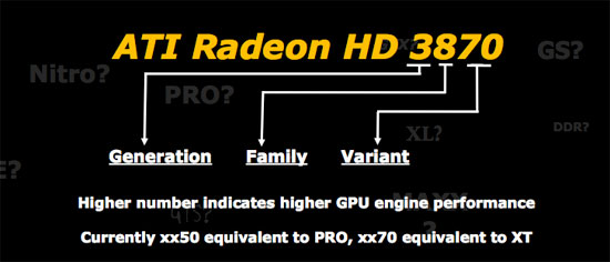
A family name, Radeon HD, followed by a four digit number. With the exception of the X2s, AMD has stuck to its naming system without fault. In fact, AMD has done such a good job with keeping the names clean that things are the way they should be: the internal codenames are more difficult to remember than the actual names of the cards (e.g. RV770 vs. Radeon HD 4870).
NVIDIA however, just hasn't gotten the hint. The GT200 launch gave us two simply named cards: the GeForce GTX 280 and GTX 260, but it didn't take long for NVIDIA to confuse the marketplace with the launch of the GeForce 9800 GTX+. I hoped that the naming silliness was limited to the older GeForce 9 GPUs, but today it extended into the GTX lineup.
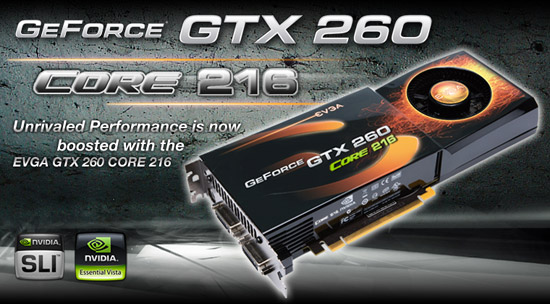
It's called the GeForce GTX 260 Core 216.
Holy nomenclature Batman
The GeForce GTX 260 Core 216's name is actually quite descriptive, albeit absurdly long. The GeForce GTX 260 part we already know from the GT200 launch, the Core 216 suffix just indicates that the GPU has 216 "cores" (also playing on Intel's new Core i7 naming for Nehalem, due out later this year). Why NVIDIA didn't just call it a GeForce GTX 265 or 270 is beyond me. To make matters worse, we'll see companies adding their own suffixes to the already extended name. For example, EVGA sent us their Core 216 called the EVGA GeForce GTX 260 Core 216 Superclocked Edition. Perhaps it's some conspiracy to increase the salary of writers who get paid by the word.
| GTX 280 | GTX 260 Core 216 | GTX 260 | 9800 GTX+ | 9800 GT | |
| Stream Processors | 240 | 216 | 192 | 128 | 112 |
| Texture Address / Filtering | 80 / 80 | 72/72 | 64 / 64 | 64 / 64 | 56 / 56 |
| ROPs | 32 | 28 | 28 | 16 | 16 |
| Core Clock | 602MHz | 576MHz | 576MHz | 738MHz | 600MHz |
| Shader Clock | 1296MHz | 1242MHz | 1242MHz | 1836MHz | 1500MHz |
| Memory Clock | 1107MHz | 999MHz | 999MHz | 1100MHz | 900MHz |
| Memory Bus Width | 512-bit | 448-bit | 448-bit | 256-bit | 256-bit |
| Frame Buffer | 1GB | 896MB | 896MB | 512MB | 512MB |
| Transistor Count | 1.4B | 1.4B | 1.4B | 754M | 754M |
| Manufacturing Process | TSMC 65nm | TSMC 65nm | TSMC 65nm | TSMC 55nm | TSMC 55nm |
| Price Point | $420 - $500 | $279 | $250 - $300 | $200 | $130 - $170 |
If you remember the diagram below from our GT200 review you'll see that a GeForce GTX 280 has ten clusters of 24 stream processors (the little blue blocks), for a total of 240 SPs or "cores". The GeForce GTX 260 has eight of those clusters (called Texture/Processor Clusters or TPCs), bringing its total up to 192 SPs. The Core 216, as you can guess, has nine clusters or 216 SPs. NVIDIA just enabled another TPC on the Core 216 (or alternatively, disabled a TPC on a GTX 280).
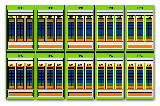
The GeForce GTX 280, 10 TPCs, 240 SPs
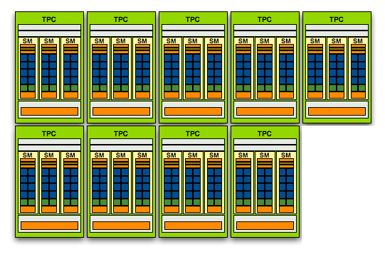
The GeForce GTX 260 Core 216, 9 TPCs, 216 SPs
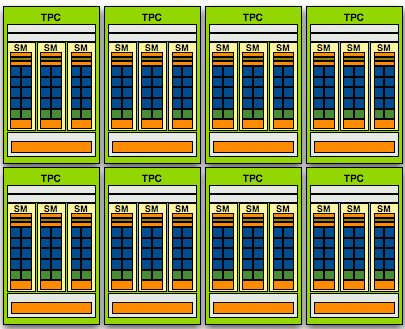
The GeForce GTX 260, 8 TPCs, 192 SPs
The extra TPC also gives the Core 216 another 8 texture address and filtering units, but the rest of the chip's makeup remains the same, even down to the clock speeds. The Core 216 runs its core, shader and memory clocks at the same frequencies as the vanilla GTX 260.
Priced at $279, the Core 216 is a direct competitor to AMD's Radeon HD 4870 - selling at a similar price. The GTX 260 will continue to exist although selling at a cheaper price point and naturally with more processing power, the GTX 280 remains unaffected.


65 Comments
View All Comments
araczynski - Wednesday, September 17, 2008 - link
it'll be quite a long while before nvidia competes again in the bank/$ game. i also got in on the two 4850's for under 300 deals when they first came out...nvidia needs to go back to the drawing board on their current chipset offerings.
Jedi2155 - Tuesday, September 16, 2008 - link
Why is that in almost every single benchmark I've seen here with Crysis, its always without AA?I think that is a important component to measure as it puts a further strain on the memory bandwidth and shows potential weaknesses of an architecture. Crysis as i've seen on some other sites seems to show the limits of a 512 MB frame buffer on the 4870 versus the GTX 260's, and I would like it if Anandtech could confirm this :).
Casper42 - Tuesday, September 16, 2008 - link
I had heard that the 55nm version of the 260 and 280 was going to be called the 270 and 290 which would explain why they decided not to use 270.Overall though I agree that they need to come up with a better naming convention. Do the same Generation/Family/Varient thing as AMD or else go back to the old naming convention and make the number tell you how many SP Cores and type of memory used and stuff, and then do the GS/GT/GTX on the end to signify the clock speed level of the card within the family.
Here, nVidia, i will do it for you.
The current cards are now named:
??? = whatever the hell you like. nVCore or GeForce or CoreForce or whatever marketing name you decide to spend way too much money thinking up.
??? 208 GTX
??? 209 GTX
??? 210 GTX
Your 55nm replacements will be the:
??? 308/309/310 GTX (Assuming they use the same memory config or if you switch to a narrower width on the memory bus, it better be GDDR5 then)
2 is your family code for current gen and 3 will be for 55nm
08-10 = number of SP Cores
GTX = high end Card
So a mid range card might be something like the ??? 206 GT
And a Cheap card could be the ??? 203 GS
Dont even have to change your internal design of the SP Cores.
And if you Tick/Tock like Intel, then the next generation after this one can
Casper42 - Tuesday, September 16, 2008 - link
Next generation after 55nm can be the 4 series and then the 45nm variant of that can be the 5 series and you now have a naming convention for the next 4 years at least.pauldovi - Tuesday, September 16, 2008 - link
Why would you have one FPS at 60.9 and the other at 61? It should either be 61 and 61 or 60.9 and 61.0. If .1 is within the margin of error you should not report FPS to this accuracy.Learn a little about significant digits!
AnnonymousCoward - Wednesday, September 17, 2008 - link
"!?!?"? Is it that big of a deal? I actually prefer dropping the ".0" for the sake of simplicity, and I'm an engineer.strikeback03 - Wednesday, September 17, 2008 - link
Could be Excel automatically throwing away trailing zeros.drebo - Tuesday, September 16, 2008 - link
The main thing keeping me from upgrading my 7900GT right now is how damn many video cards there are available. I can't tell which is better, the 9600GT, 9600GSO, 9800GT, 8800GT, etc, etc, etc, as they're all within about a $40 spread and all seem to be the same damn card.It's frustrating. I wish nVidia would stop doing this. Choose a set of price points and release four to six cards for those price points. High end ($300+), mid range ($200-$300), low end ($100-$200), multimedia ($50-100), extreme low end ($30). We don't need a card spaced every $5 through the spectrum. $50 price differences should more than suffice.
aeternitas - Wednesday, September 17, 2008 - link
Its not really that bad. All you need to do is a little reaserch about each card and you can put them in a easy list. But yes, they do need to work on nameing..Also, they come out with a handfull of cards every 9-18 months, you cant blame them for places still selling last 2 generation cards and you getting confused! Todays highend will be tomarrows midrage, and guess what? The prices will be similer. Its your job to investigate your investment.
The power... IS YOURS!
MrSpadge - Tuesday, September 16, 2008 - link
Just get a 4850 :)(.. seriously saying this while having bought a 9800GTX+ a few weeks ago and really like it)
MrS