Nehalem - Everything You Need to Know about Intel's New Architecture
by Anand Lal Shimpi on November 3, 2008 1:00 PM EST- Posted in
- CPUs
Further Power Managed Cache?
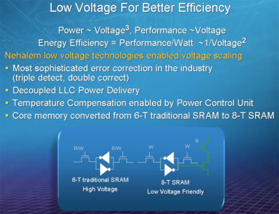
One new thing we learned about Nehalem at IDF was that Intel actually moved to a 8T (8 transistor) SRAM cell design for all of the core cache memory (L1 and L2 caches, but not L3 cache). By moving to a 8T design Intel was able to actually reduce the operating voltage of Nehalem, which in turn reduces power consumption. You may remember that Intel’s Atom team did something similar with its L1 cache:
“Instead of bumping up the voltage and sticking with a small signal array, Intel switched to a register file (1 read/1 write port). The cache now had a larger cell size (8 transistors per cell) which increased the area and footprint of the L1 instruction and data caches. The Atom floorplan had issues accommodating the larger sizes so the data cache had to be cut down from 32KB to 24KB in favor of the power benefits. We wondered why Atom had an asymmetrical L1 data and instruction cache (24KB and 32KB respectively, instead of 32KB/32KB) and it turns out that the cause was voltage.
A small signal array design based on a 6T cell has a certain minimum operating voltage, in other words it can retain state until a certain Vmin. In the L2 cache, Intel was able to use a 6T signal array design since it had inline ECC. There were other design decisions at work that prevented Intel from equipping the L1 cache with inline ECC, so the architects needed to go to a larger cell size in order to keep the operating voltage low.”
Intel states that Nehalem’s “Core memory converted from 6-T traditional SRAM to 8-T SRAM”. The only memory in the “core” of Nehalem is its L1 and L2 caches, which may help explain why the L2 cache per core is a very small 256KB. It would be costly to increase the transistor count of Nehalem’s 8MB L3 cache by 33%, but it’s also most likely not as necessary since the L3 cache and the rest of the uncore runs on its own voltage plane as I’ll get to shortly.


35 Comments
View All Comments
defter - Friday, August 22, 2008 - link
Links are 20-bit wide, regardless of encoding or whether 1,2,8,16 or 20 bits are used to tranmist the data.I wonder who is flamebaiting here, a previous poster just mentioned the correct link width, he wasn't talking about "usable speed".
rbadger - Thursday, August 21, 2008 - link
"Each QPI link is bi-directional supporting 6.4 GT/s per link. Each link is 2-bytes wide..."This is actually incorrect. Each link is 20 bits wide, not 16 (2 bytes). This information is on the slide posted directly below the paragraph.
JarredWalton - Thursday, August 21, 2008 - link
It's 20-bits but using a standard 8/10 encoding mechanism, so of the 20 bits only 16 are used to transmit data and the other four bits are (I believe) for clock signaling and/or error correction. It's the same thing we see with SATA and HyperTransport.ltcommanderdata - Thursday, August 21, 2008 - link
Since the PCU has a firmware, I wonder if it will be updatable? It would be useful if lessons learn in the power management logic of later steppings and in Westmere can be brought back to all Nehalems through a firmware update for lower power consumption or even better performance with better Turbo mode application. Although a failed or corrupt firmware update on a CPU could be very problematic.wingless - Thursday, August 21, 2008 - link
I thought about this when I read about it the first time too. Flashing your CPU could kill the power management or the whole CPU in one fell swoop!