The Radeon HD 4850 & 4870: AMD Wins at $199 and $299
by Anand Lal Shimpi & Derek Wilson on June 25, 2008 12:00 AM EST- Posted in
- GPUs
Building a RV770
We did this with NVIDIA's GT200 and it seemed to work out well, so let's start at the most basic level with AMD's RV770. Meet the Stream Processing Unit:
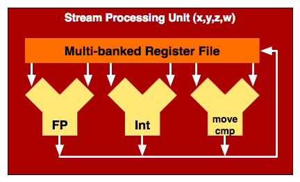
AMD's Stream Processing Unit is very similar to NVIDIA's SP in G80/G92/GT200, so similar in fact that I drew them the same way. Keep in mind that the actual inner workings of one of these units is far more complex than three ALUs but to keep things simple and consistent that's how I drew it (the actual hardware is a fused FP MUL + ADD unit, for those who care). AMD has four of these stream processing units in a processor block and they are called x, y, z or w units.
There's a fifth unit called a t-unit (the t stands for transcendental, meaning the type of operations it is capable of processing):
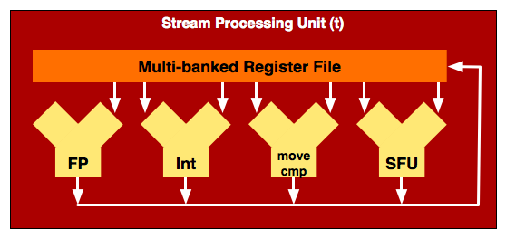
The t-unit can do everything a x,y,z or w-unit can do, but it also can do transcendental operations (represented by the SFU block in the diagram above). NVIDIA has the same functionality, it simply chooses to expose it in a different way (which we'll get to shortly). AMD considers each one of these units (x,y,z,w and t) a processing unit, and the RV770 has 800 of them (the RV670 had 320).
AMD pairs four of these stream processing units (x,y,z and w) with a t-unit and puts them together as a block, which I have decided to call a Streaming Processor (SP):
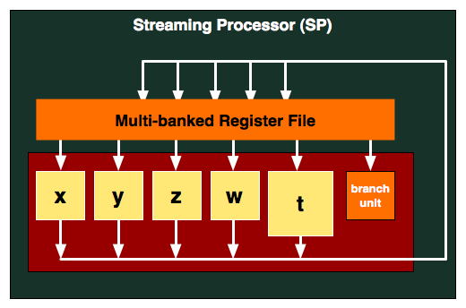
The area in red is actually the SP, but unlike one of NVIDIA's SPs, one of AMD's can handle up to five instructions at the same time. The only restriction here is that all five units have to be working on the same thread.
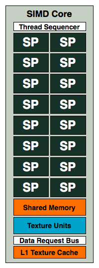
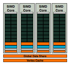
AMD then groups 16 of these SPs into something they like to call a SIMD core (AMD has less confusing, but far worse names for its architectural elements than NVIDIA):
|
AMD's SIMD Core
|
NVIDIA's SM
|
 |
 |
A SIMD core is very similar to NVIDIA's SM with a couple of exceptions:
1) There are more SPs in AMD's SIMD Core (16 vs 8)
2) The SPs are wider and can process, at peak, 5x the number of instructions as NVIDIA's SPs
3) The Instruction and Constant caches are not included in the SIMD core, AMD places them further up the ladder.
4) AMD pairs its texture units and texture cache with its SPs at the SIMD core level, while NVIDIA does it further up the ladder.
5) See the two SFUs in NVIDIA's SM? While NVIDIA has two very fast Special Function Units in its SM, AMD equips each SP with its own SFU. It's unclear which approach is actually faster given that we don't know the instruction latency or throughput of either SFU.
Note that at this point, the RV770 is really no different than the RV670 (the GPU used in the Radeon HD 3870). The next step is where AMD and NVIDIA really diverge; while NVIDIA's GT200 takes three SMs and groups them into a Texture/Processing Cluster (TPC) and then arranging 10 TPCs on its chip, AMD simply combines 10 SIMD cores:
AMD's RV670
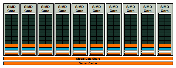
10 SIMD cores at your disposal in AMD's RV770, this is how AMD goes from competitive, to downright threatening
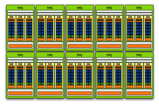
NVIDIA's GT200 Streaming Processor Array (SPA), it has fewer execution resources but more encapsulation around them, the focus here is on thread management
With 10 SIMD cores the RV770, it has 2.5x the number of execution units as a RV670. It even has more theoretical processing power than NVIDIA's GT200. If you just look at the number of concurrent instructions that can be processed on RV770 vs. GT200, the RV770's 800 execution units to GT200's 240 (+ 60 SFUs) is in a completely different league.
| NVIDIA GT200 | AMD RV770 | AMD RV670 | |
| SP Issue Width | 1-way | 5-way | 5-way |
| # of SPs | 240 | 160 | 64 |
| Worst Case Dependent Instruction Throughput | 240 | 160 | 64 |
| Maximum Scalar Instruction Throughput | 480* | 800 | 320 |
We'll be talking about efficiency and resource utilization in the coming pages, but immediately you'll notice that the RV770 (like the RV670 and R600 that came before it) has the potential to be slower than NVIDIA's architectures or significantly faster, depending entirely on how instruction or thread heavy the workload is. NVIDIA's architecture prefers tons of simple threads (one thread per SP) while AMD's architecture wants instruction heavy threads (since it can work on five instructions from a single thread at once).
NVIDIA's GeForce GTX 280
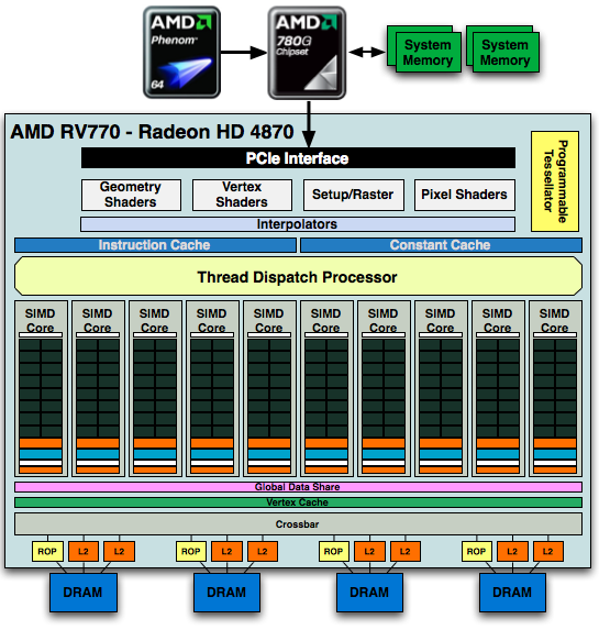
AMD's Radeon HD 4870
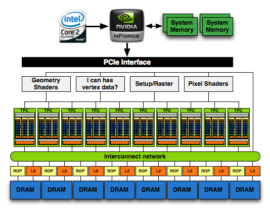
The full GPU is pretty impressive:
1) See the Instruction and Constant Caches up top? NVIDIA includes them in each SM while AMD seems to include them outside of the SIMD core clusters.
2) The RV770 only has four 64-bit memory controllers compared to the eight in GT200
3) The Programmable Tessellator is left over from the Xbox 360's GPU (and R600/RV670), unfortunately it is unused by most developers as there is no DirectX support for it yet.
4) AMD has dedicated hardware attribute interpolators, something NVIDIA's hardware shares with its special function units (SFUs).
Other than the differences we mentioned above, AMD's architecture is similar in vain to NVIDIA's, there are just a handful of design choices that set the two apart. Just like NVIDIA took its G80/G92 architecture and made it larger, AMD did the same with RV770 - it took RV670 and more than doubled its execution resources.
AMD took a bigger leap with RV770 from RV670 than NVIDIA did from G80/G92 to GT200, but it makes sense given that AMD had to be more competitive than it even was in the last generation.


215 Comments
View All Comments
natty1 - Thursday, June 26, 2008 - link
There's no good reason to pull that garbage. People assume they are seeing raw numbers when they read these reviews.DerekWilson - Sunday, June 29, 2008 - link
i don't understand what you mean by raw numbers ... these are the numbers we got in our tests ...we can't do crossfire on the nvidia board we tested and we can't do sli on the intel board we tested ...
we do have another option (skulltrail) but people seemed not to like that we went there ... and it was a pain in the ass to test with. plus fb-dimm performance leaves something to be desired.
in any case, without testing every solution in two different platforms we did the best we could in the time we had. it might be interesting to look at testing single card performance in two different platforms for all cards, but that will have to be a separate article and would be way to tough to do for a launch.
Denithor - Wednesday, June 25, 2008 - link
In Bioshock in the multiGPU section the SLI 9800GTX+ seems to fall down on the job. In all other benches this SLI beats out the GTX 280 easily, here it fails miserably. While even the SLI 8800GT beats the GTX 280. Methinks something's wrong here.jamstan - Wednesday, June 25, 2008 - link
Egg's got them for 309.99. I'm gonna run 2 4870s in CF. I planned on using a P45 board but I am wondering if the P45s X8 per card will bottleneck the bandwidth and if I should go with an X48 board instead? When I research CF all I seem to find is "losing any bandwidth at X8 versus X16 is "debateable". What I'm thinking is that 8 pipelines can handle 4GBs so if I look at the 4870s 3.6 Gbs of memory bandwidth then X8 should be able to handle the 4870 without any performance hits. It that correct or am I all wet?jamstan - Friday, June 27, 2008 - link
I contacted ATI and they said I was correct. A P45 board only running X8 per card in CF will bottleneck the massive DDR5 bandwidth of the 4870s. If you're gonna CF 2 4870s use an X38 or X48 board.SVM79 - Wednesday, June 25, 2008 - link
I created an account just to say how awesome this article was. It was really nice to see all the technical details laid out and compared to the competition. I was lucky to get in on that $150 hd4850 price at best buy last week and I am hoping the future drivers with improve performance even more. Please keep up the good work on these articles!!!DerekWilson - Sunday, June 29, 2008 - link
Wow, Anand and I are honored.We absolutely appreciate the feedback we've gotten from all of you guys (even the bad stuff cause it helps us refine our future articles).
of course we enjoy the good stuff more :-)
thanks again, everyone.
D3SI - Wednesday, June 25, 2008 - link
Long time reader, first time postergreat article, very informative
looks like the 4870 is the card to get, cant be beat at that price
and yes a lot of posters are reading way too much into it "you're biased waaa waaa boo hoo"
just get the facts from the article (thats what the charts and graphs are for) and then make your decision, if you cant do simple math and come to the conclusion yourself that the $300 card is a better buy than the $650 then you deserve to get ripped off.
joeschleprock - Wednesday, June 25, 2008 - link
nVidia just got their pussy smoked.kelectron - Wednesday, June 25, 2008 - link
a very important comparison is missing. for those who want to go in for a multi-GPU setup, the 260 SLI vs 4870 CF is a very important consideration since SLI scaling has always been better than CF, and the 260 scales very very well.in that case, if nvidia responds by reducing the price on the 260, the 260 SLI could be the real winner here. but sadly there were no 260 SLI benches.
please give us a 260 SLI vs 4870 CF review.