NVIDIA's 1.4 Billion Transistor GPU: GT200 Arrives as the GeForce GTX 280 & 260
by Anand Lal Shimpi & Derek Wilson on June 16, 2008 9:00 AM EST- Posted in
- GPUs
One-Point-Four-Billion. That's transistors folks.
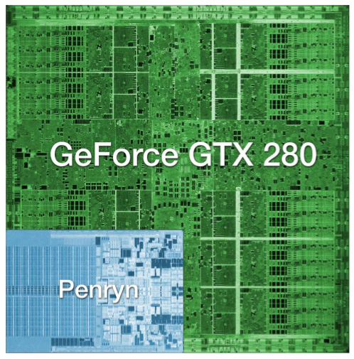
The chip is codenamed GT200 and it's the successor to NVIDIA's G80 and G92 families. Why the change in naming? The GT stands for "Graphics Tesla" and this is the second generation Graphics Tesla architecture, the first being the G80. The GT200 is launching today in two flavors, the die of the larger one is pictured below:
Um...yeah...we're reviewing that today
(this die comparison is to scale and that's a dual-core Penryn)
Let's put aside all the important considerations for a moment and bask in the glow of sheer geekdom. Intel's Montecito processor (their dual core Itanium 2) weighs in at over 1.7 billion transistors, but the vast majority of this is L3 cache (over 1.5 billion transistors for 24MB of on die memory). In contrast, the vast majority of the transistors on NVIDIA's GT200 chip are used for compute power. Whether or not NVIDIA has used these transistors well is certainly the most important consideration for consumers, but there's no reason we can't take a second to be in awe of the sheer magnitude of the hardware. This chip is packed full of logic and it is huge.
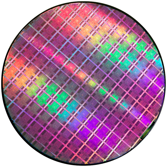
At most, 94 NVIDIA GT200 die can be produced on a single 300mm 65nm wafer from TSMC. On the other end of the spectrum, Intel can fit around 2500 45nm Atom processors on a 300mm wafer.
If the number of transistors wasn't enough to turn this thing into a dinner plate sized bit of hardware, the fact that it's fabbed on a 65nm process definitely puts it over the top. Current CPUs are at 45nm and NVIDIA's major competitor in the GPU market, AMD, has been building 55nm graphics chips for over 7 months now. With so many transistors, choosing not to shrink their manufacturing process doesn't seem to make much sense to us. Smaller fab processes offer not only the potential for faster, cooler chips, but also significantly reduce the cost of the GPU itself. Because manufacturing costs are (after ramping production) on a per wafer basis, the more dies that can be packed onto a single waffer, the less each die costs. It is likely that NVIDIA didn't want to risk any possible delays arising from manufacturing process changes on this cycle, but that seems like a risk that would have been worth taking in this case.
Instead, GT200 is the largest die TSMC has ever fabbed for production. Quite a dubious honor, and I wouldn't expect NVIDIA to really see this as something of which to be proud. Of course, that doesn't mean we can't be impressed with the sheer massiveness of the beast.
And what do we get from all these transistors? Moving up from 690M transistors of the original G80 and 754M transistors in G92 to the 1.4B transistors of GT200 is not a small tweak. One of the major new features is the ability to processes double precision floating point data in hardware (there are 30 64-bit FP units in GT200). The size of the register file for each SP array has been doubled. The promised ability of an SP to process a MAD and a MUL at the same time has been enhanced to work in more cases (G80 was supposedly able to do this, but the number of cases where it worked as advertised were extremely limited). And the number of SPs has increased from 128 on G80 to 240 with GT200. To better understand what all this means, we'll take a closer look at the differences between G80 and GT200, but first, the cards.
Clock Speeds, Pricing and HDMI Information
NVIDIA is introducing two GT200 parts today along with slightly tweaked branding. The new brand is called the GeForce GTX, and the first two cards are the GTX 280 and GTX 260.


Here's the card, say hello:
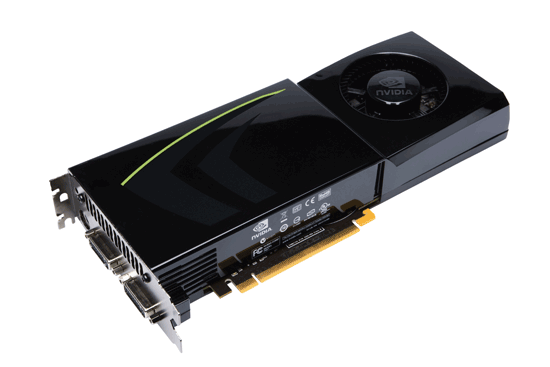
The GeForce GTX 280
It's got a little sibling too:

The GeForce GTX 260
The GeForce GTX 280 features 240 streaming processors running at 1.3GHz. It's got a 512-bit memory interface to 1GB of GDDR3 running at 2.2GHz (1107MHz core clock). The rest of the GPU runs at 602MHz.
| |
GTX 280 | GTX 260 | 9800 GX2 | 9800 GTX | 8800 GTS 512 | 8800 GT |
| Stream Processors | 240 | 192 | 256 | 128 | 128 | 112 |
| Texture Address / Filtering | 80 / 80 | 64 / 64 | 128 / 128 | 64 / 64 | 56 / 56 | 56 / 56 |
| ROPs | 32 | 28 | 32 | 16 | 16 | 16 |
| Core Clock | 602MHz | 576MHz | 600MHz | 675MHz | 650MHz | 600MHz |
| Shader Clock | 1296MHz | 1242MHz | 1500MHz | 1690MHz | 1625MHz | 1500MHz |
| Memory Clock | 1107MHz | 999MHz | 1000MHz | 1100MHz | 970MHz | 900MHz |
| Memory Bus Width | 512-bit | 448-bit | 256-bit x 2 | 256-bit | 256-bit | 256-bit |
| Frame Buffer | 1GB | 896MB | 1GB | 512MB | 512MB | 512MB |
| Transistor Count | 1.4B | 1.4B | 1.5B | 754M | 754M | 754M |
| Manufacturing Process | TSMC 65nm | TSMC 65nm | TSMC 65nm | TSMC 65nm | TSMC 65nm | TSMC 65nm |
| Price Point | $650 | $400 | $500 | $300 | $280 | $170-$230 |
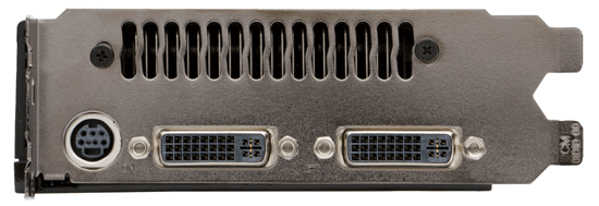
You'll need a power supply that can deliver up to 236W for the card itself and you'll need both a 6-pin and an 8-pin PCIe power connector (the board won't work with two 6-pin connectors).
The GeForce GTX 280 will retail for $650 with availability planned for June 17th.
The GTX 260 brings the total core count down to 192 by disabling two Texture/Processing Clusters on the GPU (but still maintaining more cores than any single-GPU G80/G92 based card). The SPs run slightly slower on the GTX 260 (1242MHz vs. 1296MHz, NVIDIA uses a 27MHz crystal so that's why we get these funny clock frequencies), while the memory runs at approximately 2GHz (999MHz memory clock, 1998MHz data rate). The GTX 260 also loses one of the 8 64-bit memory controllers, bringing the total memory bus down to 448-bits and total memory size down to 896MB.
The GTX 260 consumes a maximum of 183W and only needs two 6-pin power connectors. The GeForce GTX 260 will set you back $400 and should be available on June 26th.
The GTX 280's shroud, though it takes some cues from the 9800 GX2, is better engineered to allow for heat expulsion through a larger vent next to the IO ports. The 9800 GX2 didn't have a very wide opening to the outside world from which to remove heat. This resulted in the 9800 GX2 disproportionately increasing the heat of the system. Since we run our systems without cases we don't see problems like this as soon as our readers do, and we would like to thank you for pointing this out to us.
Both the GTX 260 and 280 have two dual-link DVI outputs, which can be converted to HDMI using an adapter if you'd like. You can pass SPDIF using a connector at the top of the card, which will then be passed to the HDMI output when using the DVI-HDMI adapter. For the HTPC enthusiasts out there, the GTX 280 and 260 can output the following audio formats over HDMI:
2-channel LPCM
6-channel DD bitstream
6-channel DTS bitstream
Unfortunately there's no support for 8-channel LPCM or bitstreaming of Dolby TrueHD or DTS HD-MA.


108 Comments
View All Comments
epobirs - Monday, June 16, 2008 - link
There is an important precedent that gives Nvidia good reason to not rush to a new smaller process level. Recall when ATI first became a serious player in gaming GPUs with the 9700. It was for its time a big chip pushing the limits of the process level, while Nvidia at the time was concentrating on bleeding edge technology. Nvidia's chips got stomped by ATI's in that generation, in large part because the ATI chip had far better optimization of its transistors.anartik - Monday, June 16, 2008 - link
We can agree the pricing sucks. But the point that seems to be missing is that Nvidia promised a 50% performance improvement and they delivered. The 280 delivers 45FPS vs 32FPS for the 9800GT in Assassins creed. Thats just shy of 50% (48FPS) which is a huge performance increase compared to what we have been getting the past couple years for a new card. Slap 2x280 on a card and it vaporizes the 9800 GX2 or any SLI/Xfire solution. The 9800 GX2 scales ~63% over the 9800GTX. So if you do that for a 280GX2 (or SLI) you get roughly 73 frames per second. Plus the new cards have more memory to deal with bandwidth and large textures vs the nuetered 512 on the 96/9800's and 8800GT... the reason I have held onto my 8800 GTX with 768mb. Granted I won't be rushing out and buying one tomorrow but the 280 is the fastest GPU and a x2 will be faster than any other x2 card. It's a little rediculous to think the single 280 sucks becuase it's not faster than multiple GPU's like the 9800 GX2 (although when memory counts it is).araczynski - Monday, June 16, 2008 - link
this is all they could spit out? all that noise and all those transistors and it gets its ass handed to it by the gx2 more often than not?talk about fizzle, perhaps at best it'll lower the price of the gx2 a bit.
not to mention no built in hdmi, good lord, they must've had two seperate teams working on the gtx and gx2 at the same time and just wanted to see what they could come up with separately.
Ananke - Monday, June 16, 2008 - link
I don't think many people at this forum tread understand that nVidia target is the supercomputer market. I was totally impressed from one post a month ago, where a software engineer managed to put and use 3 SLI system for magnetoresonance rendering. Nvidia and AMD /that's why they acquired ATI/ have already significant experience in multiprocessor and parallel calculation. nVidia is ahead though, since they have CUDA becoming more popular for complex calculation. A year ago Intel realized parallel processing from Sun is their biggest danger, now nVidia and Ati come too. Imagine, supercomputers build with thousands of G200 chips, and only some Intels used for mapping, instead of thousands of Xeons. nVidia thinks way more ahead just for the mere visual/gaming market. I am very very impressed, and very eager to see what ATI can do. Also, I hope Ati and Havoc will be able to offer competition to CUDA, or uniformity? Anyway, from a scientific point of view, recent developments in the graphic market make foundamental science more affordable than anytime before.Reflex - Monday, June 16, 2008 - link
Anand/Derek -I am not sure why you are comparing this chip to a Penryn or other general purpose CPU as the comparisons are meaningless. GPU's are designed very differently than CPU's, namely a high level descriptor language is used and the design is then created by a program, which is then hand tweaked by engineers. By contrast, a CPU may use a high level language, but the actual design is almost entirely done by hand, with large teams working on each sub component and literally years of tweaking. It takes Intel between five and ten years to bring a design to market, which is why there is such a push by them to keep adjusting the design and optimizing it to stretch its usefulness out as long as possible to maximize the initial investment. This simply does not happen with a GPU.
GPU's are designed to last 18-24 months as a competitive solution. nVidia and Ati cannot afford to spend even five years designing them. As a result the level of hand optimization is greatly reduced, and inefficiencies with transistors are tolerated. Typically they are produced on equipment that is already paid for by the previous, more optimized products, or contracted out to third parties(TSMC). Since the products are sold for a premium, the wasted die space is not very relevant. It is a diametrically opposed process to what you see with CPU development.
Despite how impressive it may seem to go on about 1.4 billion transisters, truthfully a modern CPU does more with far less than a modern GPU, and honestly neither nVidia nor Ati are in the same league as Intel and AMD, neither at the engineering level nor when comparing the products they put out. To an Intel engineer, this GPU is at least four times larger than it needs to be to get the performance you get out of it.
The maturation of the industry, either due to reaching a point where GPU's can do 90% of what anyone needs, or simply because power budgets get more restrictive, will come when the level of optimization required for a CPU is required for a GPU, and product cycles stretch out to 3-5 years. Then you will have a more direct comparison between the two, since the design parameters will be much more similiar.
I am not knocking nV here, btw, I'm simply calling into question why one would even compare a Penryn to a GPU, it makes no sense at all when they were designed from the ground up for different purposes, lifespans and with different transister budgets.
7Enigma - Tuesday, June 17, 2008 - link
I think what this shows is there a brute force way of doing something that while not necessarily pretty can get you to a goal. Yes compared to Intel's latest and greatest it is a grotesque abomination of wasted energy/transistors/die size, but the bottom line is it is pretty darn impressive from a CPU/GPU standpoint.I think many of us long for the days of more than 2 major competetors for each race (CPU/GPU). We've been stuck in a rut with ATI and Nvidia, AMD and Intel. Yes you have some niche products by other companies, and budget pieces being made by a host of has-beens, but really tier 1 stuff is just not being fought over by more than 2 companies.
What I want to see (complete dreamland here) is a start up from some very savvy disgruntled employees of say AMD/ATI, Intel, IBM, etc. (and don't forget possibly the most important segment, the marketing team) with some clout and a LOT of dough to say, "Screw this, we're going balls to the wall and throw the kitchen sink at the market."
I mean let's be honest here, what's another 100 watts or a billion transistors anymore? I can guarantee you every geek out there would shell out more money for a product that devestates the current competition. I don't care if it's not as frugal with the power, or as small, or as pretty, I want the speed man, gimme the speed!
Anand Lal Shimpi - Monday, June 16, 2008 - link
While I'd normally agree with you, GPUs have been getting pretty complex to design. Much of the shader multiprocessors in G80 and GT200 were designed by hand, and remember that G80 (the original predecessor to GT200) was in development for four years before its launch.The transistor comparison is a valid one, while Penryn is a very impressive design, it is so for different reasons than GT200. The size of GT200 also helps illustrate fundamental differences in approach to CPU vs. GPU design and really highlights why Intel is building Larrabee.
-A
crimson117 - Monday, June 16, 2008 - link
Because to non-engineers, they're two silicon computer chips, and 1.4 billion of anything is a lot!It also helps me to visually understand why this thing gets so hot, since it's got so much more surface area packed with transistors.
You're right that CPUs and GPUs are designed for different tasks and shouldn't be considered pure apples to apples, but then you go against your own advice and start saying how CPUs are so much more advanced, and how Intel engineers could do that in 1/4 the size of a chip. So which is it - should they be compared, or should they not be compared?
And the authors did mention how simple it could be for either company to slap the other type of chip right in with their usual type; make a Intel CPU with added GPU capabilities, or make a nVidia GPU with CPU capabilities. So there's another point where they recognize the differences but do try to illustrate the sameness.
So I'm not really sure your criticisms hold water.
Reflex - Monday, June 16, 2008 - link
You are looking for contradictions where there are none. A chip is a chip, but that does not mean that they are all designed with the same goals, budgets and time constraints. *IF* Intel devoted the resources to a GPU that they devote to a CPU, yes they could produce a product like this in a fraction of the transisters. That said, the product would take 5-10 years to design, would cost hundreds of millions of dollars to develop, and would need a lifespan of at least 5 years in the market to be worth the effort. Obviously this is not a reasonable approach in a market with such fast product turnover.My post was not an attempt to diss nV or this product, it was pointing out that the comparison of a GPU to a CPU is inane as they have completely different design constraints. You may as well compare a CPU to cache memory, or RAM or a sound processor. All have transisters, right?
It especially bothered me when they implied that nVidia has the transister budget to toss a general purpose CPU on the die. The fact is that they may have the transister budget, but they do not have the time or money available to do so, and the product would be obsolete before it ever hit the market as a result of such an attempt. It would be marrying two completely different design philosophies, and this is why the combined CPU/GPU products that are upcoming are not likely to be the strongest performers.
paydirt - Monday, June 16, 2008 - link
You all seem to be assuming that GPUs will only be used for games. If that's all you care about, then why do you whine when a GPU is made to perform well as a number cruncher (for science, for modeling/simulations)?It's the best single GPU gaming card.
It's the best widely (?) available GPU number cruncher.
For a whole system gaming GPU solution, it isn't the most cost effective.
If you're all into numbers, then why are you assigning emotions to it. It simply is what it is.