NVIDIA's 1.4 Billion Transistor GPU: GT200 Arrives as the GeForce GTX 280 & 260
by Anand Lal Shimpi & Derek Wilson on June 16, 2008 9:00 AM EST- Posted in
- GPUs
Derek Gets Technical: 15th Century Loom Technology Makes a Comeback
Because it's multithreaded...
Yes I know it's horrible, but NVIDIA has gone a bit deeper in explaining their architecture to us and they thought borrowing terminology from weaving was clever. But as much as that might make you want to roll your eyes, the explanation of how things work that is enabled is worth it.
In cloth weaving, a warp is the vertical group of parallel threads that are held taught while the weft are the threads passed through these. I suppose it makes sense, then, that NVIDIA decided to call their grouping of parallel threads to be executed on an SM a warp.

See the group of threads that hang from the top of this loom? That's called a warp.
With each SM having 8 SPs and G80 having two SMs per TPC (for a total of 16 SPs) it looked like a natural fit to execute quads across these 16 scalar units. We learned that this was not the case, but seeing the grouping of three SMs per TPC in GT200 still looked a little funny until we really learned more about how things are scheduled on NVIDIA's unified architecture. Each SM's scheduler picks a new warp to work on every clock cycle, and since the scheduler runs at half speed this ends up being every other clock cycle from the perspective of the rest of the SM. Each warp is made up of a group of 32 threads (in pixel shaders this is a group of 8 quads) that share an instruction stream (a shader program or a kernel if you're talking about GPU computing).
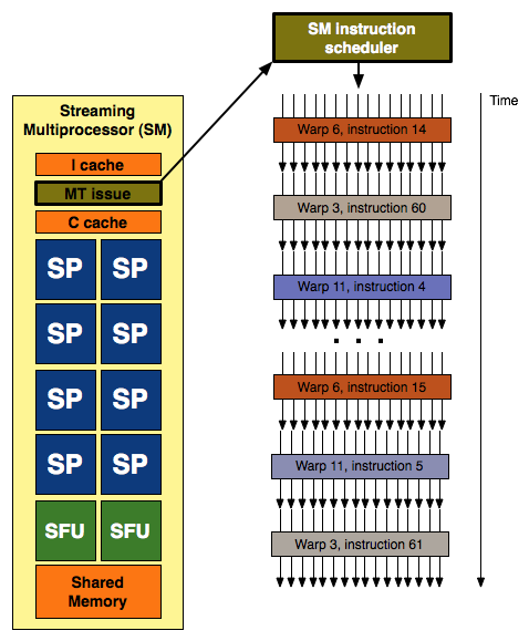
32 threads in a warp, issued in two groups of 16 threads - one such group is depicted above
Different warps built from threads executing the same shader program can follow completely independant paths down the code, but every thread within a warp must be exectuing the same instruction. This means that our branch granularity is 32 threads: every block of 32 threads (every warp) can branch independantly of all others, but if one or more threads within a warp branch in a different direction than the rest then every single thread in that warp must execute both code paths. Each threads only retains the result from the path it was supposed to follow probably by using the branch result to dynamically predicate the apporpriate path per thread. Each SM can have 32 (up from 24 in G80) warps in flight at the same time (for a total of 1024 threads in flight per SM). With 10 TPCs each containing 3 SMs, that's up to 30720 threads in flight on a GTX 280.
Each SM with it's 8 SPs and 2 SFUs is capable of processing up to 8 ops per clock (MAD (a fused floating point multiply and add) being the most complex) in the SPs and 8 ops per clock on the SFUs (which are made up of 4 floating point MUL units and other logic). Warps are executed on SMs in 2 groups of 16 threads (probably four quads for pixels) over four clock cycles.
This is where it gets interesting.
The SPs and SFUs are scheduled on alternating clock cycles from the perspective of the SM scheduler. They execute independent warps. SPs are scheduled on one clock cycle and SFUs are scheduled the next. Each is able to complete the processing of an entire warp before the next time it is scheduled, which happens to be four clocks (relative to the SPs and SFUs) after they it was scheduled with the last warp.
But wait ... aren't SMs supposed to be able to support dual-issue MAD+MUL? Well, back when G80 launched, Beyond3d did an excellent job of exploring the reality of the situation. With the fact that the SFU handles the "dual-issued" MUL and shares its time with other responsibilities like transcendental calculation and attribute interpolation, the ability of the hardware to actually accelerate cases that could take advantage of dual-issue was significantly reduced. But this scheduling revelation makes it clear that the problem is much more complex.
In order for code that could benefit from dual-issue hardware to take advantage of G80 or GT200, a warp must be scheduled on an SP for the MAD and then it must be re-scheduled on the SFU before it hits the SPs again. If the SFU is too busy handling attribute interpolation or transcendental math, then our warp will be rescheduled on the SPs to calculate the MUL and we will have lost our potential dual-issue speed up.
NVIDIA tells us that they "had some scheduling/issue problems with getting the MUL in the SFU to work consistently per clock. We fixed that in GT200." This makes perfect sense in light of what we now know about scheduling on G80/GT200. What they needed to do to improve the ability of their hardware to speed up cases where a MAD+MUL dual issue would help was to make sure that these cases were properly prioritized to execute on the SFU. We don't see MAD+MUL in every line of code, so giving these cases higher priority on the SFU than its other duties should help to optimize the utilization of the hardware. They do have to be careful not to start just running random MULs on the SFU because those special functions do still need to get done, but pushing a select subset of MULs onto the SFU (where they directly follow MADs that have just been executed on SPs) should definitely help in certain cases.
Really the main focus for NVIDIA is proper utilization and prioritization. Everything for any given frame needs to get done at some point or other, so simulating "dual-issue" shouldn't take priority over other things that need to get done that might be more important to completing the next frame. But organizing how to handle it is a big deal. Real time compilers are a big part of that, but internal thread management and scheduling in an architechure this wide also cannot be ignored. NVIDIA says they can now get 93-94% efficiency from their "dual-issue" implementation in directed tests and that this is significantly higher than on G80. Real world results will be lower, but the thing to remember is that the goal is simply to make maximally efficient use of the hardware availalbe. Just because the SFU isn't assisting in a MAD+MUL every clock doesn't mean it isn't doing something important.
This whole situation leaves us with mixed feelings. The hardware itself is not capable of "dual-issue" as it is understood in an architectural sense. The obfuscation of graphics hardware technology in a competitive industry has been the norm for the past decade, and we can accept this. We would prefer to know what the hardware is actually doing, but we are more than happy to have an explanation of something as a hardware feature where the hardware merely simulates the effect a specific architectural design has. But in the case where the hardware doesn't perform in nearly the same way as it would if the feature had actually been implemented as a hardware feature, we just can't help but be a little disappointed.
And we are conflicted about this because NVIDIA's design is actually very elegant. Attribute interpolation will always need to be done, and having hardware set aside for complex math is also very useful. But rather than making a dedicated fixed function interpolator or doing taylor expansion of complex math on SPs, NVIDIA built hardware that could serve both purposes and that had time left over to help offload some well placed MULs within the instruction stream of running programs.
If NVIDIA had been as open about their architecture as Intel is about their CPU designs, we could not have helped but to be impressed by this. The "missing MUL" wouldn't have been seen as a problem with NVIDIA's dual-issue "hardware"; we would have been praising NVIDIA's ability to schedule and multitask the different units within their SMs in order to improve utilization.


108 Comments
View All Comments
epobirs - Monday, June 16, 2008 - link
There is an important precedent that gives Nvidia good reason to not rush to a new smaller process level. Recall when ATI first became a serious player in gaming GPUs with the 9700. It was for its time a big chip pushing the limits of the process level, while Nvidia at the time was concentrating on bleeding edge technology. Nvidia's chips got stomped by ATI's in that generation, in large part because the ATI chip had far better optimization of its transistors.anartik - Monday, June 16, 2008 - link
We can agree the pricing sucks. But the point that seems to be missing is that Nvidia promised a 50% performance improvement and they delivered. The 280 delivers 45FPS vs 32FPS for the 9800GT in Assassins creed. Thats just shy of 50% (48FPS) which is a huge performance increase compared to what we have been getting the past couple years for a new card. Slap 2x280 on a card and it vaporizes the 9800 GX2 or any SLI/Xfire solution. The 9800 GX2 scales ~63% over the 9800GTX. So if you do that for a 280GX2 (or SLI) you get roughly 73 frames per second. Plus the new cards have more memory to deal with bandwidth and large textures vs the nuetered 512 on the 96/9800's and 8800GT... the reason I have held onto my 8800 GTX with 768mb. Granted I won't be rushing out and buying one tomorrow but the 280 is the fastest GPU and a x2 will be faster than any other x2 card. It's a little rediculous to think the single 280 sucks becuase it's not faster than multiple GPU's like the 9800 GX2 (although when memory counts it is).araczynski - Monday, June 16, 2008 - link
this is all they could spit out? all that noise and all those transistors and it gets its ass handed to it by the gx2 more often than not?talk about fizzle, perhaps at best it'll lower the price of the gx2 a bit.
not to mention no built in hdmi, good lord, they must've had two seperate teams working on the gtx and gx2 at the same time and just wanted to see what they could come up with separately.
Ananke - Monday, June 16, 2008 - link
I don't think many people at this forum tread understand that nVidia target is the supercomputer market. I was totally impressed from one post a month ago, where a software engineer managed to put and use 3 SLI system for magnetoresonance rendering. Nvidia and AMD /that's why they acquired ATI/ have already significant experience in multiprocessor and parallel calculation. nVidia is ahead though, since they have CUDA becoming more popular for complex calculation. A year ago Intel realized parallel processing from Sun is their biggest danger, now nVidia and Ati come too. Imagine, supercomputers build with thousands of G200 chips, and only some Intels used for mapping, instead of thousands of Xeons. nVidia thinks way more ahead just for the mere visual/gaming market. I am very very impressed, and very eager to see what ATI can do. Also, I hope Ati and Havoc will be able to offer competition to CUDA, or uniformity? Anyway, from a scientific point of view, recent developments in the graphic market make foundamental science more affordable than anytime before.Reflex - Monday, June 16, 2008 - link
Anand/Derek -I am not sure why you are comparing this chip to a Penryn or other general purpose CPU as the comparisons are meaningless. GPU's are designed very differently than CPU's, namely a high level descriptor language is used and the design is then created by a program, which is then hand tweaked by engineers. By contrast, a CPU may use a high level language, but the actual design is almost entirely done by hand, with large teams working on each sub component and literally years of tweaking. It takes Intel between five and ten years to bring a design to market, which is why there is such a push by them to keep adjusting the design and optimizing it to stretch its usefulness out as long as possible to maximize the initial investment. This simply does not happen with a GPU.
GPU's are designed to last 18-24 months as a competitive solution. nVidia and Ati cannot afford to spend even five years designing them. As a result the level of hand optimization is greatly reduced, and inefficiencies with transistors are tolerated. Typically they are produced on equipment that is already paid for by the previous, more optimized products, or contracted out to third parties(TSMC). Since the products are sold for a premium, the wasted die space is not very relevant. It is a diametrically opposed process to what you see with CPU development.
Despite how impressive it may seem to go on about 1.4 billion transisters, truthfully a modern CPU does more with far less than a modern GPU, and honestly neither nVidia nor Ati are in the same league as Intel and AMD, neither at the engineering level nor when comparing the products they put out. To an Intel engineer, this GPU is at least four times larger than it needs to be to get the performance you get out of it.
The maturation of the industry, either due to reaching a point where GPU's can do 90% of what anyone needs, or simply because power budgets get more restrictive, will come when the level of optimization required for a CPU is required for a GPU, and product cycles stretch out to 3-5 years. Then you will have a more direct comparison between the two, since the design parameters will be much more similiar.
I am not knocking nV here, btw, I'm simply calling into question why one would even compare a Penryn to a GPU, it makes no sense at all when they were designed from the ground up for different purposes, lifespans and with different transister budgets.
7Enigma - Tuesday, June 17, 2008 - link
I think what this shows is there a brute force way of doing something that while not necessarily pretty can get you to a goal. Yes compared to Intel's latest and greatest it is a grotesque abomination of wasted energy/transistors/die size, but the bottom line is it is pretty darn impressive from a CPU/GPU standpoint.I think many of us long for the days of more than 2 major competetors for each race (CPU/GPU). We've been stuck in a rut with ATI and Nvidia, AMD and Intel. Yes you have some niche products by other companies, and budget pieces being made by a host of has-beens, but really tier 1 stuff is just not being fought over by more than 2 companies.
What I want to see (complete dreamland here) is a start up from some very savvy disgruntled employees of say AMD/ATI, Intel, IBM, etc. (and don't forget possibly the most important segment, the marketing team) with some clout and a LOT of dough to say, "Screw this, we're going balls to the wall and throw the kitchen sink at the market."
I mean let's be honest here, what's another 100 watts or a billion transistors anymore? I can guarantee you every geek out there would shell out more money for a product that devestates the current competition. I don't care if it's not as frugal with the power, or as small, or as pretty, I want the speed man, gimme the speed!
Anand Lal Shimpi - Monday, June 16, 2008 - link
While I'd normally agree with you, GPUs have been getting pretty complex to design. Much of the shader multiprocessors in G80 and GT200 were designed by hand, and remember that G80 (the original predecessor to GT200) was in development for four years before its launch.The transistor comparison is a valid one, while Penryn is a very impressive design, it is so for different reasons than GT200. The size of GT200 also helps illustrate fundamental differences in approach to CPU vs. GPU design and really highlights why Intel is building Larrabee.
-A
crimson117 - Monday, June 16, 2008 - link
Because to non-engineers, they're two silicon computer chips, and 1.4 billion of anything is a lot!It also helps me to visually understand why this thing gets so hot, since it's got so much more surface area packed with transistors.
You're right that CPUs and GPUs are designed for different tasks and shouldn't be considered pure apples to apples, but then you go against your own advice and start saying how CPUs are so much more advanced, and how Intel engineers could do that in 1/4 the size of a chip. So which is it - should they be compared, or should they not be compared?
And the authors did mention how simple it could be for either company to slap the other type of chip right in with their usual type; make a Intel CPU with added GPU capabilities, or make a nVidia GPU with CPU capabilities. So there's another point where they recognize the differences but do try to illustrate the sameness.
So I'm not really sure your criticisms hold water.
Reflex - Monday, June 16, 2008 - link
You are looking for contradictions where there are none. A chip is a chip, but that does not mean that they are all designed with the same goals, budgets and time constraints. *IF* Intel devoted the resources to a GPU that they devote to a CPU, yes they could produce a product like this in a fraction of the transisters. That said, the product would take 5-10 years to design, would cost hundreds of millions of dollars to develop, and would need a lifespan of at least 5 years in the market to be worth the effort. Obviously this is not a reasonable approach in a market with such fast product turnover.My post was not an attempt to diss nV or this product, it was pointing out that the comparison of a GPU to a CPU is inane as they have completely different design constraints. You may as well compare a CPU to cache memory, or RAM or a sound processor. All have transisters, right?
It especially bothered me when they implied that nVidia has the transister budget to toss a general purpose CPU on the die. The fact is that they may have the transister budget, but they do not have the time or money available to do so, and the product would be obsolete before it ever hit the market as a result of such an attempt. It would be marrying two completely different design philosophies, and this is why the combined CPU/GPU products that are upcoming are not likely to be the strongest performers.
paydirt - Monday, June 16, 2008 - link
You all seem to be assuming that GPUs will only be used for games. If that's all you care about, then why do you whine when a GPU is made to perform well as a number cruncher (for science, for modeling/simulations)?It's the best single GPU gaming card.
It's the best widely (?) available GPU number cruncher.
For a whole system gaming GPU solution, it isn't the most cost effective.
If you're all into numbers, then why are you assigning emotions to it. It simply is what it is.