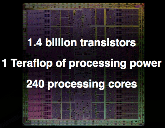
NVIDIA's 1.4 Billion Transistor GPU: GT200 Arrives as the GeForce GTX 280 & 260
by Anand Lal Shimpi & Derek Wilson on June 16, 2008 9:00 AM EST- Posted in
- GPUs
Overclocked and 4GB of GDDR3 per Card: Tesla 10P
Now let's say that you want to get some real work done with NVIDIA's GT200 GPU but that 1.4 billion transistor chip just isn't enough. NVIDIA does have an answer for you, in the form of an overclocked GT200 with the 240 SPs running at 1.5GHz (up from 1.3GHz in the GTX 280) and with a full 4GB of GDDR3 memory on-board.
Today NVIDIA is also announcing their next generation Tesla product based on GT200 (called a T10P when used on Tesla for some reason). The workstation graphics guys will have to wait a while for a GT200 Quadro unfortunately. This new Tesla is similar to the older model in that it has much more RAM and no IO ports. The server version is also clocked higher than the desktop part because fan noise isn't an issue and data centers have lower ambient temperatures than some corner of an office under a desk.
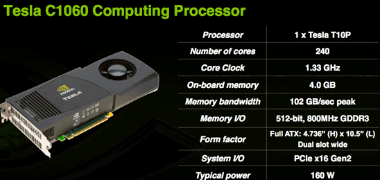
The Tesla C1060 has an entire 4GB of RAM on board. This is obviously very large and will do well to accomodate the large scale scientific computing apps it is targeted at. This card is designed for use in workstations and is the little brother to the new monster server that is also being announced today.
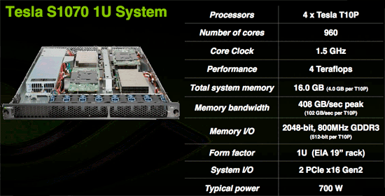
The Tesla S1070 is a 1U server containing essentially 4 C1060 cards for a total of 16GBs of RAM on 960 SPs. This server, like the older version, connects to a server via a PCIe cable and is designed to run code written for CUDA at incredible speeds. With 120 double precision IEEE 754r floating point units in combination with the 960 single precision IEEE 754 units, this server is a viable option for many more projects than the previous Tesla hardware which was only capable of single precision floating point.
Though we don't have an application to benchmark the double precision floating point hardware on GT200 yet, NVIDIA states that a GT200 can roughly match an 8 core Xeon system in DP performance. This would put the S1070 on par with a 32 way Xeon setup at less than 700W. Needless to say, single precision code runs much much faster and can outpace hundreds of traditional CPUs in parallel.
While these servers are expensive (though we don't have pricing), they are cheap compared to the alternatives currently out there. The fact that CUDA code can be implemented and tested on any of the 70 million NVIDIA G80+ GPUs currently in people's hands means that developer already have a platform to test and debug code on before committing to the Tesla solution. On top of that, schools are beginning to adopt CUDA as a teaching tool for parallel computing. As CUDA gains acceptance and the benefits of GPU computing are realized, more and more major markets will take interest.
The graphics card is no longer a toy. The combination of CUDA's academic acceptance as a teaching tool and the availability of 64-bit floating point in GT200 make GPUs a mission critical computing tool that will act as a truly disruptive technology. Not only will many major markets that depend on high performance floating-point processing realize this, but every consumer with an NVIDIA graphics card will be able to take advantage of hundreds of gigaflops of performance from CUDA based consumer applications.
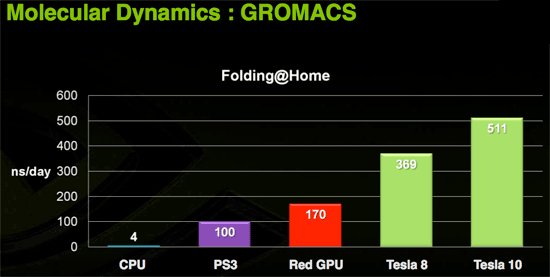
Today we have folding@home and soon we'll have Elemental's transcoder. Imagine the audio and video processing capabilities of a PC if the GPU were actively used in software like ProTools and Premier. Open source programs could easily best the processing capabilities of many solutions with dedicated hardware for these types of applications.
Of course, the major limiter to the adoption of this technology is that it is vendor specific. If NVIDIA put the time in (or enlisted help) to make CUDA an ANSI or ISO standard extention to a programming language, we would could really start to get excited. Beyond that, the holy grail would be a unification of virtualized instruction sets creating a standard low level "assembly" interface for GPU computing allowing CUDA to compile to one target and run on any graphics card. Sort of an x86 for massively parallel work.
Right now CUDA compiles to PTX, NVIDIA's virtual instruction set, and there is no reason someone couldn't write a CUDA compiler to target AMD's equivalent CAL (or even to develop a PTX to CAL wrapper that allowed AMD GPUs to run compiled CUDA code). Unfortunately, NVIDIA doesn't want to invest money and resources in extending functionality to AMD and AMD doesn't want to invest money and resources into bolstering an NVIDIA owned technology (that could theoretically radically change to cripple AMD's hardware support in future versions). While standards and cooperation are a great idea, the competition in this market is such that neither NVIDIA nor AMD are looking to take a chance on benefiting the consumer if there is any risk of strenthening the competition (even in spite of weakening the industry).


108 Comments
View All Comments
epobirs - Monday, June 16, 2008 - link
There is an important precedent that gives Nvidia good reason to not rush to a new smaller process level. Recall when ATI first became a serious player in gaming GPUs with the 9700. It was for its time a big chip pushing the limits of the process level, while Nvidia at the time was concentrating on bleeding edge technology. Nvidia's chips got stomped by ATI's in that generation, in large part because the ATI chip had far better optimization of its transistors.anartik - Monday, June 16, 2008 - link
We can agree the pricing sucks. But the point that seems to be missing is that Nvidia promised a 50% performance improvement and they delivered. The 280 delivers 45FPS vs 32FPS for the 9800GT in Assassins creed. Thats just shy of 50% (48FPS) which is a huge performance increase compared to what we have been getting the past couple years for a new card. Slap 2x280 on a card and it vaporizes the 9800 GX2 or any SLI/Xfire solution. The 9800 GX2 scales ~63% over the 9800GTX. So if you do that for a 280GX2 (or SLI) you get roughly 73 frames per second. Plus the new cards have more memory to deal with bandwidth and large textures vs the nuetered 512 on the 96/9800's and 8800GT... the reason I have held onto my 8800 GTX with 768mb. Granted I won't be rushing out and buying one tomorrow but the 280 is the fastest GPU and a x2 will be faster than any other x2 card. It's a little rediculous to think the single 280 sucks becuase it's not faster than multiple GPU's like the 9800 GX2 (although when memory counts it is).araczynski - Monday, June 16, 2008 - link
this is all they could spit out? all that noise and all those transistors and it gets its ass handed to it by the gx2 more often than not?talk about fizzle, perhaps at best it'll lower the price of the gx2 a bit.
not to mention no built in hdmi, good lord, they must've had two seperate teams working on the gtx and gx2 at the same time and just wanted to see what they could come up with separately.
Ananke - Monday, June 16, 2008 - link
I don't think many people at this forum tread understand that nVidia target is the supercomputer market. I was totally impressed from one post a month ago, where a software engineer managed to put and use 3 SLI system for magnetoresonance rendering. Nvidia and AMD /that's why they acquired ATI/ have already significant experience in multiprocessor and parallel calculation. nVidia is ahead though, since they have CUDA becoming more popular for complex calculation. A year ago Intel realized parallel processing from Sun is their biggest danger, now nVidia and Ati come too. Imagine, supercomputers build with thousands of G200 chips, and only some Intels used for mapping, instead of thousands of Xeons. nVidia thinks way more ahead just for the mere visual/gaming market. I am very very impressed, and very eager to see what ATI can do. Also, I hope Ati and Havoc will be able to offer competition to CUDA, or uniformity? Anyway, from a scientific point of view, recent developments in the graphic market make foundamental science more affordable than anytime before.Reflex - Monday, June 16, 2008 - link
Anand/Derek -I am not sure why you are comparing this chip to a Penryn or other general purpose CPU as the comparisons are meaningless. GPU's are designed very differently than CPU's, namely a high level descriptor language is used and the design is then created by a program, which is then hand tweaked by engineers. By contrast, a CPU may use a high level language, but the actual design is almost entirely done by hand, with large teams working on each sub component and literally years of tweaking. It takes Intel between five and ten years to bring a design to market, which is why there is such a push by them to keep adjusting the design and optimizing it to stretch its usefulness out as long as possible to maximize the initial investment. This simply does not happen with a GPU.
GPU's are designed to last 18-24 months as a competitive solution. nVidia and Ati cannot afford to spend even five years designing them. As a result the level of hand optimization is greatly reduced, and inefficiencies with transistors are tolerated. Typically they are produced on equipment that is already paid for by the previous, more optimized products, or contracted out to third parties(TSMC). Since the products are sold for a premium, the wasted die space is not very relevant. It is a diametrically opposed process to what you see with CPU development.
Despite how impressive it may seem to go on about 1.4 billion transisters, truthfully a modern CPU does more with far less than a modern GPU, and honestly neither nVidia nor Ati are in the same league as Intel and AMD, neither at the engineering level nor when comparing the products they put out. To an Intel engineer, this GPU is at least four times larger than it needs to be to get the performance you get out of it.
The maturation of the industry, either due to reaching a point where GPU's can do 90% of what anyone needs, or simply because power budgets get more restrictive, will come when the level of optimization required for a CPU is required for a GPU, and product cycles stretch out to 3-5 years. Then you will have a more direct comparison between the two, since the design parameters will be much more similiar.
I am not knocking nV here, btw, I'm simply calling into question why one would even compare a Penryn to a GPU, it makes no sense at all when they were designed from the ground up for different purposes, lifespans and with different transister budgets.
7Enigma - Tuesday, June 17, 2008 - link
I think what this shows is there a brute force way of doing something that while not necessarily pretty can get you to a goal. Yes compared to Intel's latest and greatest it is a grotesque abomination of wasted energy/transistors/die size, but the bottom line is it is pretty darn impressive from a CPU/GPU standpoint.I think many of us long for the days of more than 2 major competetors for each race (CPU/GPU). We've been stuck in a rut with ATI and Nvidia, AMD and Intel. Yes you have some niche products by other companies, and budget pieces being made by a host of has-beens, but really tier 1 stuff is just not being fought over by more than 2 companies.
What I want to see (complete dreamland here) is a start up from some very savvy disgruntled employees of say AMD/ATI, Intel, IBM, etc. (and don't forget possibly the most important segment, the marketing team) with some clout and a LOT of dough to say, "Screw this, we're going balls to the wall and throw the kitchen sink at the market."
I mean let's be honest here, what's another 100 watts or a billion transistors anymore? I can guarantee you every geek out there would shell out more money for a product that devestates the current competition. I don't care if it's not as frugal with the power, or as small, or as pretty, I want the speed man, gimme the speed!
Anand Lal Shimpi - Monday, June 16, 2008 - link
While I'd normally agree with you, GPUs have been getting pretty complex to design. Much of the shader multiprocessors in G80 and GT200 were designed by hand, and remember that G80 (the original predecessor to GT200) was in development for four years before its launch.The transistor comparison is a valid one, while Penryn is a very impressive design, it is so for different reasons than GT200. The size of GT200 also helps illustrate fundamental differences in approach to CPU vs. GPU design and really highlights why Intel is building Larrabee.
-A
crimson117 - Monday, June 16, 2008 - link
Because to non-engineers, they're two silicon computer chips, and 1.4 billion of anything is a lot!It also helps me to visually understand why this thing gets so hot, since it's got so much more surface area packed with transistors.
You're right that CPUs and GPUs are designed for different tasks and shouldn't be considered pure apples to apples, but then you go against your own advice and start saying how CPUs are so much more advanced, and how Intel engineers could do that in 1/4 the size of a chip. So which is it - should they be compared, or should they not be compared?
And the authors did mention how simple it could be for either company to slap the other type of chip right in with their usual type; make a Intel CPU with added GPU capabilities, or make a nVidia GPU with CPU capabilities. So there's another point where they recognize the differences but do try to illustrate the sameness.
So I'm not really sure your criticisms hold water.
Reflex - Monday, June 16, 2008 - link
You are looking for contradictions where there are none. A chip is a chip, but that does not mean that they are all designed with the same goals, budgets and time constraints. *IF* Intel devoted the resources to a GPU that they devote to a CPU, yes they could produce a product like this in a fraction of the transisters. That said, the product would take 5-10 years to design, would cost hundreds of millions of dollars to develop, and would need a lifespan of at least 5 years in the market to be worth the effort. Obviously this is not a reasonable approach in a market with such fast product turnover.My post was not an attempt to diss nV or this product, it was pointing out that the comparison of a GPU to a CPU is inane as they have completely different design constraints. You may as well compare a CPU to cache memory, or RAM or a sound processor. All have transisters, right?
It especially bothered me when they implied that nVidia has the transister budget to toss a general purpose CPU on the die. The fact is that they may have the transister budget, but they do not have the time or money available to do so, and the product would be obsolete before it ever hit the market as a result of such an attempt. It would be marrying two completely different design philosophies, and this is why the combined CPU/GPU products that are upcoming are not likely to be the strongest performers.
paydirt - Monday, June 16, 2008 - link
You all seem to be assuming that GPUs will only be used for games. If that's all you care about, then why do you whine when a GPU is made to perform well as a number cruncher (for science, for modeling/simulations)?It's the best single GPU gaming card.
It's the best widely (?) available GPU number cruncher.
For a whole system gaming GPU solution, it isn't the most cost effective.
If you're all into numbers, then why are you assigning emotions to it. It simply is what it is.