NVIDIA's 1.4 Billion Transistor GPU: GT200 Arrives as the GeForce GTX 280 & 260
by Anand Lal Shimpi & Derek Wilson on June 16, 2008 9:00 AM EST- Posted in
- GPUs
Building NVIDIA's GT200
Here's a Streaming Processor, NVIDIA calls it an SP:
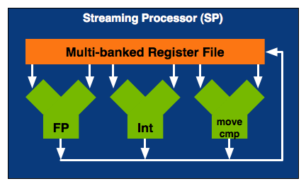
NVIDIA calls an individual SP a single processing core, which is actually true. It is a fully pipelined, single-issue, in-order microprocessor complete with two ALUs and a FPU. An SP doesn't have any cache, so it's not particularly great at anything other than cranking through tons of mathematical operations. Since an SP spends most of its time working on pixel or vertex data, the fact that it doesn't have a cache doesn't really matter. Aside from name similarities, one NVIDIA SP is a lot like a very simplified version of a SPE in the Cell microprocessor (or maybe the SPE is like a really simple version of one of NVIDIA's SMs, which we'll get to in a minute). While a single SPE in Cell has seven execution units, a single NVIDIA SP only has three.
By itself a SP is fairly useless, but NVIDIA builds GPUs and if you add up enough of these little monsters you can start to get something productive given that graphics rendering is a highly parallelizable task.
Here's a Streaming Multiprocessor, which NVIDIA abbreviates as SM:

A SM is an array of SPs, eight to be specific, along with two more processors called Special Function Units (SFUs). Each SFU has four FP multiply units which are used for transcendental operations (e.g. sin, cosin) and interpolation, the latter being used in some of the calculations for things like anisotropic texture filtering. Although NVIDIA isn't specific in saying so, we assume that each SFU is also a fully pipelined, single-issue, in-order microprocessor. There's a MT issue unit that dispatches instructions to all of the SPs and SFUs in the group.
In addition to the processor cores in a SM, there's a very small instruction cache, a read only data cache and a 16KB read/write shared memory. These cache sizes are kept purposefully small because unlike a conventional desktop microprocessor, the datasets we're trying to cache here are small. Each SP ends up working on an individual pixel and despite the move to 32-bit floating point values, there's only so much data associated with a single pixel. The 16KB memory is akin to Cell's local stores in that it's not a cache, but a software-managed data store so that latency is always predictable. With this many cores in a single SM, control and predictability and very important to making the whole thing work efficiently.
Take one more step back and you've got a Texture/Processor Cluster (TPC):
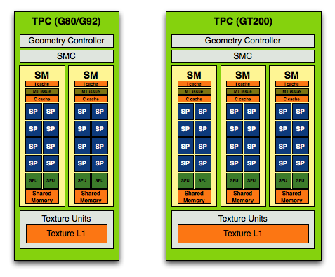
The G80/G92 TPC (left) vs. the GT200 TPC (right)
NVIDIA purposefully designed its GPU architecture to be modular, so a single TPC can be made up of any number of SMs. In the G80 architecture it was made up of two SMs but with the GT200 architecture it now has three SMs.
The components of the TPC however haven't changed; a TPC is made up of SMs, some control logic and a texture block. Remember that a SM is a total of 8 SPs and 2 SFUs, so that brings the total up to 24 SPs and 6 SFUs (must...not...type...STFU) per cluster in GT200 (up from 16 SPs and 4 SFUs in G80). The texture block includes texture addressing and filtering logic as well as a L1 texture cache.
The modular theme continues with the Streaming Processor Array (SPA) that is composed of a number of TPCs:
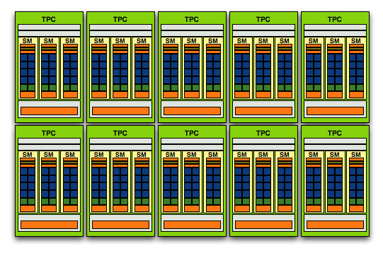
The GT200 SPA, that's 240 SPs in there if you want to count them
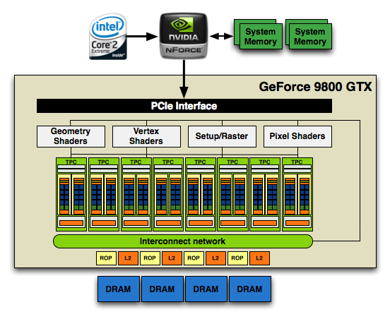
In G80 the SPA was made up of 8 TPCs, but with GT200 we've moved up to 10. Note that each TPC now has 3 SMs vs. 2, so the overall processing power of GT200 has increased by 87.5% over G80.
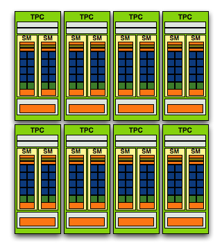
And here's G80/G92, only 128 SPs thanks to two SMs per TPC and 8 TPCs
At the front end of the GPU we've got schedulers and control logic to distribute workloads to the entire array of processing cores. At the other end we've got L2 texture caches and rasterization processors that handle final filtering and output of data to the frame buffer.
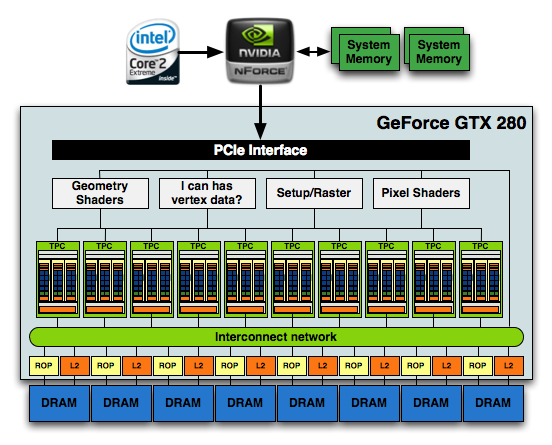
The culmination of all of this is that the new GT200 GPU, the heart of the GeForce GTX 280 and 260, features 240 SPs, 160KB of local memory, an even smaller amount of cache and is built on TSMC's 65nm process using 1.4 billion transistors.
1.4 Billion Transistors. It wants vertex data. Really bad.
754 Million Transistors
There are more transistors in this chip than there are people in China, and it's the largest, most compute-dense chip we've ever reviewed.


108 Comments
View All Comments
tkrushing - Wednesday, June 18, 2008 - link
Say what you want about this guy but this is partially true which is why AMD/ATI is in the position they have been. They are slowly climbing out of that hole they've been in though. Would have been nice to see 4870x2 hit the market first. As we know competition = less prices for everyone!hk690 - Tuesday, June 17, 2008 - link
I would love to kick you hard in the face, breaking it. Then I'd cut your stomach open with a chainsaw, exposing your intestines. Then I'd cut your windpipe in two with a boxcutter. Then I'd tie you to the back of a pickup truck, and drag you, until your useless fucking corpse was torn to a million fucking useless, bloody, and gory pieces.
Hopefully you'll get what's coming to you. Fucking bitch
http://www.youtube.com/watch?v=XNAFUpDTy3M">http://www.youtube.com/watch?v=XNAFUpDTy3M
I wish you a truly painful, bloody, gory and agonizing death, cunt
7Enigma - Wednesday, June 18, 2008 - link
Anand, I'm all for free speech and such, but this guy is going a bit far. I read these articles at work frequently and once the dreaded C-word is used I'm paranoid I'm being watched.Mr Roboto - Thursday, June 19, 2008 - link
I thought those comments would be deleted already. I'm sure no one cares if they are. I don't know what that person is so mad about .hk690 - Tuesday, June 17, 2008 - link
Die painfully okay? Prefearbly by getting crushed to death in a garbage compactor, by getting your face cut to ribbons with a pocketknife, your head cracked open with a baseball bat, your stomach sliced open and your entrails spilled out, and your eyeballs ripped out of their sockets. Fucking bitch
Mr Roboto - Wednesday, June 18, 2008 - link
Ouch.. Looks like you hit a nerve with AMD\ATI's marketing team!bobsmith1492 - Monday, June 16, 2008 - link
The main benefit from the 280 is the reduced power at idle! If I read the graph right, at idle the 9800 takes ~150W more than the 280 while at idle. Since that's where computers spend the majority of their time, depending on how much you game, that can be a significant cost.kilkennycat - Monday, June 16, 2008 - link
Maybe you should look at the GT200 series from the point of view of nvidia's GPGPU customers - the academic researchers, technology companies requiring fast number-cruching available on the desktop, the professionals in graphics-effects and computer animation - not necessarily real-time, but as quick as possible... The CUDA-using crew. The Tesla initative. This is an explosively-expanding and highly profitable business for nVidia - far more profitable per unit than any home desktop graphics application. An in-depth analysis by Anandtech of what the GT200 architecture brings to these markets over and above the current G8xx/G9xx architecture would be highly appreciated. I have a very strong suspicion that sales of the GT2xx series to the (ultra-rich) home user who has to have the latest and greatest graphics card is just another way of paying the development bills and not the true focus for this particular architecture or product line.nVidia is strongly rumored to be working on the true 2nd-gen Dx10.x product family, to be introduced early next year. Considering the size of the GTX280 silicon, I would expect them to transition the 65nm GTX280 GPU to either TSMC's 45nm or 55nm process before the end of 2008 to prove out the process with this size of device, then in 2009 introduce their true 2nd-gen GPU/GPGPU family on this latter process. A variant on the Intel "tic-toc" process strategy.
strikeback03 - Tuesday, June 17, 2008 - link
But look at the primary audience of this site. Whatever nvidia's intentions are for the GT280, I'm guessing more people here are interested in gaming than in subsidizing research.Wirmish - Tuesday, June 17, 2008 - link
"...requiring fast number-cruching available on the desktop..."GTX 260 = 715 GFLOPS
GTX 280 = 933 GFLOPS
HD 4850 = 1000 GFLOPS
HD 4870 = 1200 GFLOPS
4870 X2 = 2400 GFLOPS
Take a look here: http://tinyurl.com/5jwym5">http://tinyurl.com/5jwym5