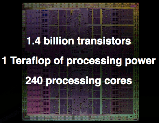
NVIDIA's 1.4 Billion Transistor GPU: GT200 Arrives as the GeForce GTX 280 & 260
by Anand Lal Shimpi & Derek Wilson on June 16, 2008 9:00 AM EST- Posted in
- GPUs
Overclocked and 4GB of GDDR3 per Card: Tesla 10P
Now let's say that you want to get some real work done with NVIDIA's GT200 GPU but that 1.4 billion transistor chip just isn't enough. NVIDIA does have an answer for you, in the form of an overclocked GT200 with the 240 SPs running at 1.5GHz (up from 1.3GHz in the GTX 280) and with a full 4GB of GDDR3 memory on-board.
Today NVIDIA is also announcing their next generation Tesla product based on GT200 (called a T10P when used on Tesla for some reason). The workstation graphics guys will have to wait a while for a GT200 Quadro unfortunately. This new Tesla is similar to the older model in that it has much more RAM and no IO ports. The server version is also clocked higher than the desktop part because fan noise isn't an issue and data centers have lower ambient temperatures than some corner of an office under a desk.
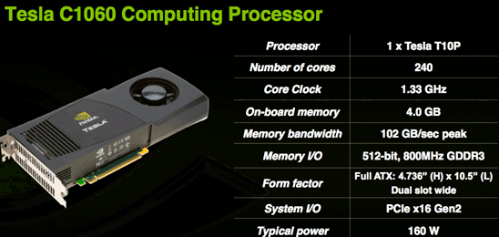
The Tesla C1060 has an entire 4GB of RAM on board. This is obviously very large and will do well to accomodate the large scale scientific computing apps it is targeted at. This card is designed for use in workstations and is the little brother to the new monster server that is also being announced today.
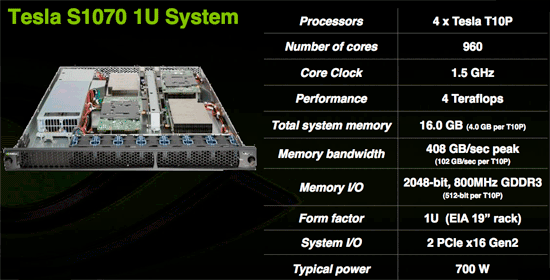
The Tesla S1070 is a 1U server containing essentially 4 C1060 cards for a total of 16GBs of RAM on 960 SPs. This server, like the older version, connects to a server via a PCIe cable and is designed to run code written for CUDA at incredible speeds. With 120 double precision IEEE 754r floating point units in combination with the 960 single precision IEEE 754 units, this server is a viable option for many more projects than the previous Tesla hardware which was only capable of single precision floating point.
Though we don't have an application to benchmark the double precision floating point hardware on GT200 yet, NVIDIA states that a GT200 can roughly match an 8 core Xeon system in DP performance. This would put the S1070 on par with a 32 way Xeon setup at less than 700W. Needless to say, single precision code runs much much faster and can outpace hundreds of traditional CPUs in parallel.
While these servers are expensive (though we don't have pricing), they are cheap compared to the alternatives currently out there. The fact that CUDA code can be implemented and tested on any of the 70 million NVIDIA G80+ GPUs currently in people's hands means that developer already have a platform to test and debug code on before committing to the Tesla solution. On top of that, schools are beginning to adopt CUDA as a teaching tool for parallel computing. As CUDA gains acceptance and the benefits of GPU computing are realized, more and more major markets will take interest.
The graphics card is no longer a toy. The combination of CUDA's academic acceptance as a teaching tool and the availability of 64-bit floating point in GT200 make GPUs a mission critical computing tool that will act as a truly disruptive technology. Not only will many major markets that depend on high performance floating-point processing realize this, but every consumer with an NVIDIA graphics card will be able to take advantage of hundreds of gigaflops of performance from CUDA based consumer applications.
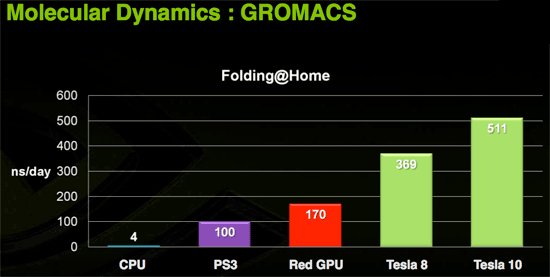
Today we have folding@home and soon we'll have Elemental's transcoder. Imagine the audio and video processing capabilities of a PC if the GPU were actively used in software like ProTools and Premier. Open source programs could easily best the processing capabilities of many solutions with dedicated hardware for these types of applications.
Of course, the major limiter to the adoption of this technology is that it is vendor specific. If NVIDIA put the time in (or enlisted help) to make CUDA an ANSI or ISO standard extention to a programming language, we would could really start to get excited. Beyond that, the holy grail would be a unification of virtualized instruction sets creating a standard low level "assembly" interface for GPU computing allowing CUDA to compile to one target and run on any graphics card. Sort of an x86 for massively parallel work.
Right now CUDA compiles to PTX, NVIDIA's virtual instruction set, and there is no reason someone couldn't write a CUDA compiler to target AMD's equivalent CAL (or even to develop a PTX to CAL wrapper that allowed AMD GPUs to run compiled CUDA code). Unfortunately, NVIDIA doesn't want to invest money and resources in extending functionality to AMD and AMD doesn't want to invest money and resources into bolstering an NVIDIA owned technology (that could theoretically radically change to cripple AMD's hardware support in future versions). While standards and cooperation are a great idea, the competition in this market is such that neither NVIDIA nor AMD are looking to take a chance on benefiting the consumer if there is any risk of strenthening the competition (even in spite of weakening the industry).


108 Comments
View All Comments
skiboysteve - Tuesday, June 17, 2008 - link
FANTASTIC write up on fine-grained TMT. I was unaware about this threading technique and was always thinking of this in class or whenever someone would talk about hyperthreading. this technique was literaly in my head for well over a year and I didn't know what it was called or that it even had a name. I always thought there had to be a more elegant way than hyperthreading to do multithreading down at the chip level without doing the OS style time slicing.i was sitting there wondering how the hell the schedule and run these SPs and then bam whole page about it
really appreciate the effort that goes into researching the core of these chips. i know not everyone likes it but for guys that are educated and work in the field its really interesting
DerekWilson - Tuesday, June 17, 2008 - link
remember though that this type of fine-grained TMT only has payoffs in systems running millions of threads concurrently.on an OS you'll see hundreds or even thousands of threads on heavily used systems, but there still wouldn't be enough concurrent action to justify this type of architecture for general purpose computing.
of course, as developers push towards an effort to thread their code as much as possible, who knows what architectures might be worth exploring on the desktop ...
coder0000 - Tuesday, June 17, 2008 - link
Very well written! A couple of points:1) Last week at WWDC Apple announced OpenCL as an alternative to CUDA. It's a C99 based HLL for creating compute kernels that can be deployed to GPU's and CPU's. Today Khronos officially announced a working group for this, and NV is a part of the committee. As such, your wish for an industry standardized compute language similar to CUDA that runs on all platforms and vendors HW may not be so far off.
2) I believe your interpretation of how multiple threads simultaneously execute in an SM is incorrect. Per thread context switching is not free, and you would never be able to execute a different thread every cycle in the manner described. There is far too much context that needs to be swapped out, and there would be significant power implications for doing that, in addition to the latency. Instead, I believe what NV is claiming is that any given SP executes a single thread. All threads in the SM can all be a single warp, but you can also have multiple threads (one per SP) all executing simultaneously in an SM.
DerekWilson - Tuesday, June 17, 2008 - link
1) I haven't had a good chance to look at OpenCL, but I certainly hope that if it's everything everyone is saying it is in the comments here that it takes off in a bigger way than CUDA :-)2) it does not context switch per thread -- warps define a context, and you have 32 threads grouped together. these threads all share the same instruction stream, which is why if threads in a warp take different directions on a branch all 32 threds must follow both paths.
NVIDIA has flat out stated that every schedule clock a new warp is scheduled and that it takes 4 clock cycles to process one warp on an SM. For both of these to be true, we conclude that the scheduler alternates scheduling SPs and SFUs on altenating clocks which means the SPs would be scheduled every 4 clocks relative to itself.
On 8 SPs per SM, you some how need to execute 32 threads in 4 clock cycles. This makes sense if you execute 4 threads per SP in some way. The details at this point are fuzzy though.
regardless, if an SP executes 4 different threads from the same warp, there is no need to context switch to execute any of these threads -- again, threads in the same warp share context.
skiboysteve - Tuesday, June 17, 2008 - link
could be a large explanation of the 2x register file size. and remember that the SP doesn't have to worry about the context switch, the SM handles having the data in the right placeanandtech02148 - Monday, June 16, 2008 - link
From this conclusion, Amd seems to be the shrewd player, let nvidia and intel duke it out in the high voltage, heat, meaningless speed gpu while Amd can pull something like its first dualcore or athlon64 for the win.this new beast from Nvidia will have how many developers making games for it right away? i'm guestimating maybe 2yrs-4yrs down the road we'll see a decent title that take full advantage of this hardware.
by then Amd will have something of a midrange that can more than handle the games.
2 things nvidia could work on that it already has, the ps3 market, and small graphic devices to improve profits. shrink the ps3 gpu further so Sony can shrink it's machinel and sell more.
PrinceGaz - Monday, June 16, 2008 - link
The GT200 core may be a technical masterpeice in terms of actually making something that big which is fully functional on GTX280 cards, but it seems to me the penalty of fabbing it at 65nm negates much of the benefits of such a wide GPU.They've had to drop the clock speeds throughout presumably because of the ridiculous amount of heat such a large core generates, which means the ~60% performance advantage in current games over the G80 core at similar clock-speeds is somewhat reduced.
Given that ATI are not producing their 55nm cores in AMD's fabs but instead are getting them churned out reliably elsewhere, nVidia have made a mistake this time around in having their high-end product rely on previous-generation fabrication as it makes it run too hot to allow the clock-speeds needed for it to be the product it should be. There is always a risk in transitioning to a smaller fab technology, and nVidia suffered badly in the past by doing so too early, but with a chip the size of the GT200, they really should have gone to 55nm even if it meant a delay of a month or three, whilst the smaller cut-down derivatives were rolled out first.
ekpyr - Monday, June 16, 2008 - link
Great article, but what about the microstuttering issues present in Nvidia's 9800GX2 cards (both SLI and Quad-SLI)? There is very little discussion on this, but I've seen some benchmarks where the FPS floor is 4fps with the 9800GX2s. Can you add a subjective review of whether or not the actual gameplay is smoother with the GTX280s across these games? Aggregate numbers may say one thing, but I've returned a 9800 GX2 Quad-SLI setup because it was unable to handle the incredible amount of texture loading that was done in Age of Conan (2560x1600 4xAA 'High' settings = 4fps). The 8800 GTX Tri-SLI configuration I am currently using is more resilient to microstuttering with its increased bus and memory capacities, but I'm very curious about the GTX280s and their increased memory and bus on texture-heavy games like Age of Conan.DerekWilson - Monday, June 16, 2008 - link
the only game that came close to having this issue with quad sli for us was oblivion.in that game at high res lag and stutter are unbearable and the game is unplayable.
we didn't notice any stuttering issues with a single GX2.
i'm working on some analysis tools to show details like this better in future articles.
TheJian - Monday, June 16, 2008 - link
I find it humorous that nobody discusses the fact that the shrink has already taped out and will likely be out in two months or just after. This humongous chip was only released so that when AMD releases in the next few weeks they will be behind still in single GPU cards. This is basically what Intel does to AMD every time AMD has a better chip. For all intents and purposes this is a PAPER release of what will come in 2-2.5 months (In Intel's case they just show you what will be out 6 months from now, and a large portion of people don't buy an AMD because Intel might be ahead by xmas...LOL - works like a charm every time AMD is ahead). THE DIE SHRUNK CHIP! Most likely with faster speeds. I suspect they'll come with "ULTRA" version first (and stick it on top of the price heap, so as to not kill all FAT cards in the channel already) and then filter down as these big suckers leave the channel. That's if they even plan to sell more than a few of these to begin withat 65nm. It's only out there so AMD won't look any good in two weeks.MIND SHARE is everything, which is why Intel's KING of the paper launch when behind strategy. They've even went to doing it for all chips no matter what now. Nehalem scores 6 months before availability. AMD's marketers have no clue an should be fired. You have to play the same DIRTY game as your enemy or you've already lost. If AMD had half a brain in their head they'd paper launch an ultra or 2x4870 version for the same reason...LOL. Then claim "our 4870x2 makes nvidia look like crap for $600"...ROFL. Who cares when it's available, just say it. Having said that, Nvidia will wipe the floor with them in 2 months anyway on a 2xGTX280 that's die shrunk. Which is all they are doing today...BUYING TIME!