NVIDIA's 1.4 Billion Transistor GPU: GT200 Arrives as the GeForce GTX 280 & 260
by Anand Lal Shimpi & Derek Wilson on June 16, 2008 9:00 AM EST- Posted in
- GPUs
Building NVIDIA's GT200
Here's a Streaming Processor, NVIDIA calls it an SP:
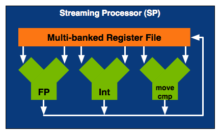
NVIDIA calls an individual SP a single processing core, which is actually true. It is a fully pipelined, single-issue, in-order microprocessor complete with two ALUs and a FPU. An SP doesn't have any cache, so it's not particularly great at anything other than cranking through tons of mathematical operations. Since an SP spends most of its time working on pixel or vertex data, the fact that it doesn't have a cache doesn't really matter. Aside from name similarities, one NVIDIA SP is a lot like a very simplified version of a SPE in the Cell microprocessor (or maybe the SPE is like a really simple version of one of NVIDIA's SMs, which we'll get to in a minute). While a single SPE in Cell has seven execution units, a single NVIDIA SP only has three.
By itself a SP is fairly useless, but NVIDIA builds GPUs and if you add up enough of these little monsters you can start to get something productive given that graphics rendering is a highly parallelizable task.
Here's a Streaming Multiprocessor, which NVIDIA abbreviates as SM:

A SM is an array of SPs, eight to be specific, along with two more processors called Special Function Units (SFUs). Each SFU has four FP multiply units which are used for transcendental operations (e.g. sin, cosin) and interpolation, the latter being used in some of the calculations for things like anisotropic texture filtering. Although NVIDIA isn't specific in saying so, we assume that each SFU is also a fully pipelined, single-issue, in-order microprocessor. There's a MT issue unit that dispatches instructions to all of the SPs and SFUs in the group.
In addition to the processor cores in a SM, there's a very small instruction cache, a read only data cache and a 16KB read/write shared memory. These cache sizes are kept purposefully small because unlike a conventional desktop microprocessor, the datasets we're trying to cache here are small. Each SP ends up working on an individual pixel and despite the move to 32-bit floating point values, there's only so much data associated with a single pixel. The 16KB memory is akin to Cell's local stores in that it's not a cache, but a software-managed data store so that latency is always predictable. With this many cores in a single SM, control and predictability and very important to making the whole thing work efficiently.
Take one more step back and you've got a Texture/Processor Cluster (TPC):
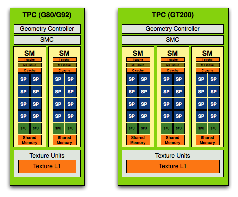
The G80/G92 TPC (left) vs. the GT200 TPC (right)
NVIDIA purposefully designed its GPU architecture to be modular, so a single TPC can be made up of any number of SMs. In the G80 architecture it was made up of two SMs but with the GT200 architecture it now has three SMs.
The components of the TPC however haven't changed; a TPC is made up of SMs, some control logic and a texture block. Remember that a SM is a total of 8 SPs and 2 SFUs, so that brings the total up to 24 SPs and 6 SFUs (must...not...type...STFU) per cluster in GT200 (up from 16 SPs and 4 SFUs in G80). The texture block includes texture addressing and filtering logic as well as a L1 texture cache.
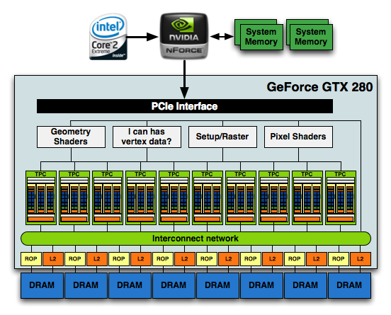
The modular theme continues with the Streaming Processor Array (SPA) that is composed of a number of TPCs:
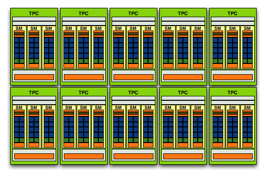
The GT200 SPA, that's 240 SPs in there if you want to count them
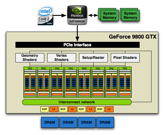
In G80 the SPA was made up of 8 TPCs, but with GT200 we've moved up to 10. Note that each TPC now has 3 SMs vs. 2, so the overall processing power of GT200 has increased by 87.5% over G80.
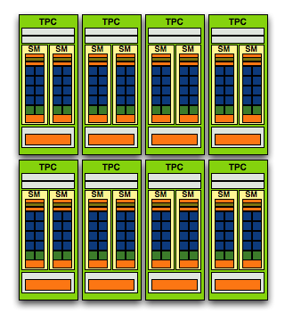
And here's G80/G92, only 128 SPs thanks to two SMs per TPC and 8 TPCs
At the front end of the GPU we've got schedulers and control logic to distribute workloads to the entire array of processing cores. At the other end we've got L2 texture caches and rasterization processors that handle final filtering and output of data to the frame buffer.
The culmination of all of this is that the new GT200 GPU, the heart of the GeForce GTX 280 and 260, features 240 SPs, 160KB of local memory, an even smaller amount of cache and is built on TSMC's 65nm process using 1.4 billion transistors.
1.4 Billion Transistors. It wants vertex data. Really bad.
754 Million Transistors
There are more transistors in this chip than there are people in China, and it's the largest, most compute-dense chip we've ever reviewed.


108 Comments
View All Comments
skiboysteve - Tuesday, June 17, 2008 - link
FANTASTIC write up on fine-grained TMT. I was unaware about this threading technique and was always thinking of this in class or whenever someone would talk about hyperthreading. this technique was literaly in my head for well over a year and I didn't know what it was called or that it even had a name. I always thought there had to be a more elegant way than hyperthreading to do multithreading down at the chip level without doing the OS style time slicing.i was sitting there wondering how the hell the schedule and run these SPs and then bam whole page about it
really appreciate the effort that goes into researching the core of these chips. i know not everyone likes it but for guys that are educated and work in the field its really interesting
DerekWilson - Tuesday, June 17, 2008 - link
remember though that this type of fine-grained TMT only has payoffs in systems running millions of threads concurrently.on an OS you'll see hundreds or even thousands of threads on heavily used systems, but there still wouldn't be enough concurrent action to justify this type of architecture for general purpose computing.
of course, as developers push towards an effort to thread their code as much as possible, who knows what architectures might be worth exploring on the desktop ...
coder0000 - Tuesday, June 17, 2008 - link
Very well written! A couple of points:1) Last week at WWDC Apple announced OpenCL as an alternative to CUDA. It's a C99 based HLL for creating compute kernels that can be deployed to GPU's and CPU's. Today Khronos officially announced a working group for this, and NV is a part of the committee. As such, your wish for an industry standardized compute language similar to CUDA that runs on all platforms and vendors HW may not be so far off.
2) I believe your interpretation of how multiple threads simultaneously execute in an SM is incorrect. Per thread context switching is not free, and you would never be able to execute a different thread every cycle in the manner described. There is far too much context that needs to be swapped out, and there would be significant power implications for doing that, in addition to the latency. Instead, I believe what NV is claiming is that any given SP executes a single thread. All threads in the SM can all be a single warp, but you can also have multiple threads (one per SP) all executing simultaneously in an SM.
DerekWilson - Tuesday, June 17, 2008 - link
1) I haven't had a good chance to look at OpenCL, but I certainly hope that if it's everything everyone is saying it is in the comments here that it takes off in a bigger way than CUDA :-)2) it does not context switch per thread -- warps define a context, and you have 32 threads grouped together. these threads all share the same instruction stream, which is why if threads in a warp take different directions on a branch all 32 threds must follow both paths.
NVIDIA has flat out stated that every schedule clock a new warp is scheduled and that it takes 4 clock cycles to process one warp on an SM. For both of these to be true, we conclude that the scheduler alternates scheduling SPs and SFUs on altenating clocks which means the SPs would be scheduled every 4 clocks relative to itself.
On 8 SPs per SM, you some how need to execute 32 threads in 4 clock cycles. This makes sense if you execute 4 threads per SP in some way. The details at this point are fuzzy though.
regardless, if an SP executes 4 different threads from the same warp, there is no need to context switch to execute any of these threads -- again, threads in the same warp share context.
skiboysteve - Tuesday, June 17, 2008 - link
could be a large explanation of the 2x register file size. and remember that the SP doesn't have to worry about the context switch, the SM handles having the data in the right placeanandtech02148 - Monday, June 16, 2008 - link
From this conclusion, Amd seems to be the shrewd player, let nvidia and intel duke it out in the high voltage, heat, meaningless speed gpu while Amd can pull something like its first dualcore or athlon64 for the win.this new beast from Nvidia will have how many developers making games for it right away? i'm guestimating maybe 2yrs-4yrs down the road we'll see a decent title that take full advantage of this hardware.
by then Amd will have something of a midrange that can more than handle the games.
2 things nvidia could work on that it already has, the ps3 market, and small graphic devices to improve profits. shrink the ps3 gpu further so Sony can shrink it's machinel and sell more.
PrinceGaz - Monday, June 16, 2008 - link
The GT200 core may be a technical masterpeice in terms of actually making something that big which is fully functional on GTX280 cards, but it seems to me the penalty of fabbing it at 65nm negates much of the benefits of such a wide GPU.They've had to drop the clock speeds throughout presumably because of the ridiculous amount of heat such a large core generates, which means the ~60% performance advantage in current games over the G80 core at similar clock-speeds is somewhat reduced.
Given that ATI are not producing their 55nm cores in AMD's fabs but instead are getting them churned out reliably elsewhere, nVidia have made a mistake this time around in having their high-end product rely on previous-generation fabrication as it makes it run too hot to allow the clock-speeds needed for it to be the product it should be. There is always a risk in transitioning to a smaller fab technology, and nVidia suffered badly in the past by doing so too early, but with a chip the size of the GT200, they really should have gone to 55nm even if it meant a delay of a month or three, whilst the smaller cut-down derivatives were rolled out first.
ekpyr - Monday, June 16, 2008 - link
Great article, but what about the microstuttering issues present in Nvidia's 9800GX2 cards (both SLI and Quad-SLI)? There is very little discussion on this, but I've seen some benchmarks where the FPS floor is 4fps with the 9800GX2s. Can you add a subjective review of whether or not the actual gameplay is smoother with the GTX280s across these games? Aggregate numbers may say one thing, but I've returned a 9800 GX2 Quad-SLI setup because it was unable to handle the incredible amount of texture loading that was done in Age of Conan (2560x1600 4xAA 'High' settings = 4fps). The 8800 GTX Tri-SLI configuration I am currently using is more resilient to microstuttering with its increased bus and memory capacities, but I'm very curious about the GTX280s and their increased memory and bus on texture-heavy games like Age of Conan.DerekWilson - Monday, June 16, 2008 - link
the only game that came close to having this issue with quad sli for us was oblivion.in that game at high res lag and stutter are unbearable and the game is unplayable.
we didn't notice any stuttering issues with a single GX2.
i'm working on some analysis tools to show details like this better in future articles.
TheJian - Monday, June 16, 2008 - link
I find it humorous that nobody discusses the fact that the shrink has already taped out and will likely be out in two months or just after. This humongous chip was only released so that when AMD releases in the next few weeks they will be behind still in single GPU cards. This is basically what Intel does to AMD every time AMD has a better chip. For all intents and purposes this is a PAPER release of what will come in 2-2.5 months (In Intel's case they just show you what will be out 6 months from now, and a large portion of people don't buy an AMD because Intel might be ahead by xmas...LOL - works like a charm every time AMD is ahead). THE DIE SHRUNK CHIP! Most likely with faster speeds. I suspect they'll come with "ULTRA" version first (and stick it on top of the price heap, so as to not kill all FAT cards in the channel already) and then filter down as these big suckers leave the channel. That's if they even plan to sell more than a few of these to begin withat 65nm. It's only out there so AMD won't look any good in two weeks.MIND SHARE is everything, which is why Intel's KING of the paper launch when behind strategy. They've even went to doing it for all chips no matter what now. Nehalem scores 6 months before availability. AMD's marketers have no clue an should be fired. You have to play the same DIRTY game as your enemy or you've already lost. If AMD had half a brain in their head they'd paper launch an ultra or 2x4870 version for the same reason...LOL. Then claim "our 4870x2 makes nvidia look like crap for $600"...ROFL. Who cares when it's available, just say it. Having said that, Nvidia will wipe the floor with them in 2 months anyway on a 2xGTX280 that's die shrunk. Which is all they are doing today...BUYING TIME!