NVIDIA's 1.4 Billion Transistor GPU: GT200 Arrives as the GeForce GTX 280 & 260
by Anand Lal Shimpi & Derek Wilson on June 16, 2008 9:00 AM EST- Posted in
- GPUs
One-Point-Four-Billion. That's transistors folks.
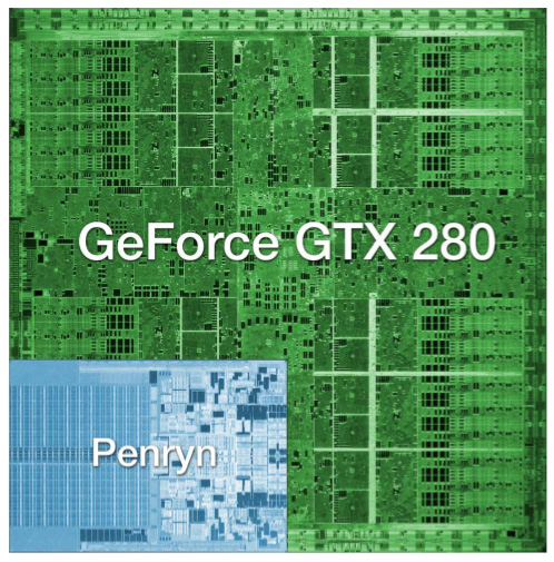
The chip is codenamed GT200 and it's the successor to NVIDIA's G80 and G92 families. Why the change in naming? The GT stands for "Graphics Tesla" and this is the second generation Graphics Tesla architecture, the first being the G80. The GT200 is launching today in two flavors, the die of the larger one is pictured below:
Um...yeah...we're reviewing that today
(this die comparison is to scale and that's a dual-core Penryn)
Let's put aside all the important considerations for a moment and bask in the glow of sheer geekdom. Intel's Montecito processor (their dual core Itanium 2) weighs in at over 1.7 billion transistors, but the vast majority of this is L3 cache (over 1.5 billion transistors for 24MB of on die memory). In contrast, the vast majority of the transistors on NVIDIA's GT200 chip are used for compute power. Whether or not NVIDIA has used these transistors well is certainly the most important consideration for consumers, but there's no reason we can't take a second to be in awe of the sheer magnitude of the hardware. This chip is packed full of logic and it is huge.
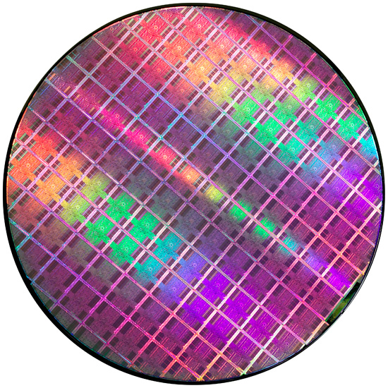
At most, 94 NVIDIA GT200 die can be produced on a single 300mm 65nm wafer from TSMC. On the other end of the spectrum, Intel can fit around 2500 45nm Atom processors on a 300mm wafer.
If the number of transistors wasn't enough to turn this thing into a dinner plate sized bit of hardware, the fact that it's fabbed on a 65nm process definitely puts it over the top. Current CPUs are at 45nm and NVIDIA's major competitor in the GPU market, AMD, has been building 55nm graphics chips for over 7 months now. With so many transistors, choosing not to shrink their manufacturing process doesn't seem to make much sense to us. Smaller fab processes offer not only the potential for faster, cooler chips, but also significantly reduce the cost of the GPU itself. Because manufacturing costs are (after ramping production) on a per wafer basis, the more dies that can be packed onto a single waffer, the less each die costs. It is likely that NVIDIA didn't want to risk any possible delays arising from manufacturing process changes on this cycle, but that seems like a risk that would have been worth taking in this case.
Instead, GT200 is the largest die TSMC has ever fabbed for production. Quite a dubious honor, and I wouldn't expect NVIDIA to really see this as something of which to be proud. Of course, that doesn't mean we can't be impressed with the sheer massiveness of the beast.
And what do we get from all these transistors? Moving up from 690M transistors of the original G80 and 754M transistors in G92 to the 1.4B transistors of GT200 is not a small tweak. One of the major new features is the ability to processes double precision floating point data in hardware (there are 30 64-bit FP units in GT200). The size of the register file for each SP array has been doubled. The promised ability of an SP to process a MAD and a MUL at the same time has been enhanced to work in more cases (G80 was supposedly able to do this, but the number of cases where it worked as advertised were extremely limited). And the number of SPs has increased from 128 on G80 to 240 with GT200. To better understand what all this means, we'll take a closer look at the differences between G80 and GT200, but first, the cards.
Clock Speeds, Pricing and HDMI Information
NVIDIA is introducing two GT200 parts today along with slightly tweaked branding. The new brand is called the GeForce GTX, and the first two cards are the GTX 280 and GTX 260.


Here's the card, say hello:
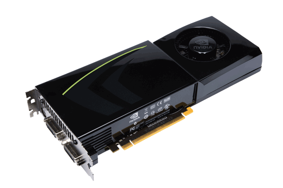
The GeForce GTX 280
It's got a little sibling too:

The GeForce GTX 260
The GeForce GTX 280 features 240 streaming processors running at 1.3GHz. It's got a 512-bit memory interface to 1GB of GDDR3 running at 2.2GHz (1107MHz core clock). The rest of the GPU runs at 602MHz.
| |
GTX 280 | GTX 260 | 9800 GX2 | 9800 GTX | 8800 GTS 512 | 8800 GT |
| Stream Processors | 240 | 192 | 256 | 128 | 128 | 112 |
| Texture Address / Filtering | 80 / 80 | 64 / 64 | 128 / 128 | 64 / 64 | 56 / 56 | 56 / 56 |
| ROPs | 32 | 28 | 32 | 16 | 16 | 16 |
| Core Clock | 602MHz | 576MHz | 600MHz | 675MHz | 650MHz | 600MHz |
| Shader Clock | 1296MHz | 1242MHz | 1500MHz | 1690MHz | 1625MHz | 1500MHz |
| Memory Clock | 1107MHz | 999MHz | 1000MHz | 1100MHz | 970MHz | 900MHz |
| Memory Bus Width | 512-bit | 448-bit | 256-bit x 2 | 256-bit | 256-bit | 256-bit |
| Frame Buffer | 1GB | 896MB | 1GB | 512MB | 512MB | 512MB |
| Transistor Count | 1.4B | 1.4B | 1.5B | 754M | 754M | 754M |
| Manufacturing Process | TSMC 65nm | TSMC 65nm | TSMC 65nm | TSMC 65nm | TSMC 65nm | TSMC 65nm |
| Price Point | $650 | $400 | $500 | $300 | $280 | $170-$230 |
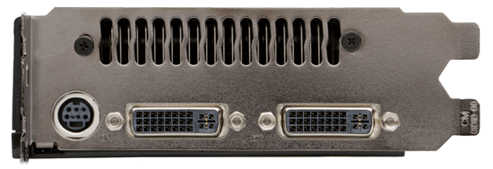
You'll need a power supply that can deliver up to 236W for the card itself and you'll need both a 6-pin and an 8-pin PCIe power connector (the board won't work with two 6-pin connectors).
The GeForce GTX 280 will retail for $650 with availability planned for June 17th.
The GTX 260 brings the total core count down to 192 by disabling two Texture/Processing Clusters on the GPU (but still maintaining more cores than any single-GPU G80/G92 based card). The SPs run slightly slower on the GTX 260 (1242MHz vs. 1296MHz, NVIDIA uses a 27MHz crystal so that's why we get these funny clock frequencies), while the memory runs at approximately 2GHz (999MHz memory clock, 1998MHz data rate). The GTX 260 also loses one of the 8 64-bit memory controllers, bringing the total memory bus down to 448-bits and total memory size down to 896MB.
The GTX 260 consumes a maximum of 183W and only needs two 6-pin power connectors. The GeForce GTX 260 will set you back $400 and should be available on June 26th.
The GTX 280's shroud, though it takes some cues from the 9800 GX2, is better engineered to allow for heat expulsion through a larger vent next to the IO ports. The 9800 GX2 didn't have a very wide opening to the outside world from which to remove heat. This resulted in the 9800 GX2 disproportionately increasing the heat of the system. Since we run our systems without cases we don't see problems like this as soon as our readers do, and we would like to thank you for pointing this out to us.
Both the GTX 260 and 280 have two dual-link DVI outputs, which can be converted to HDMI using an adapter if you'd like. You can pass SPDIF using a connector at the top of the card, which will then be passed to the HDMI output when using the DVI-HDMI adapter. For the HTPC enthusiasts out there, the GTX 280 and 260 can output the following audio formats over HDMI:
2-channel LPCM
6-channel DD bitstream
6-channel DTS bitstream
Unfortunately there's no support for 8-channel LPCM or bitstreaming of Dolby TrueHD or DTS HD-MA.


108 Comments
View All Comments
skiboysteve - Tuesday, June 17, 2008 - link
FANTASTIC write up on fine-grained TMT. I was unaware about this threading technique and was always thinking of this in class or whenever someone would talk about hyperthreading. this technique was literaly in my head for well over a year and I didn't know what it was called or that it even had a name. I always thought there had to be a more elegant way than hyperthreading to do multithreading down at the chip level without doing the OS style time slicing.i was sitting there wondering how the hell the schedule and run these SPs and then bam whole page about it
really appreciate the effort that goes into researching the core of these chips. i know not everyone likes it but for guys that are educated and work in the field its really interesting
DerekWilson - Tuesday, June 17, 2008 - link
remember though that this type of fine-grained TMT only has payoffs in systems running millions of threads concurrently.on an OS you'll see hundreds or even thousands of threads on heavily used systems, but there still wouldn't be enough concurrent action to justify this type of architecture for general purpose computing.
of course, as developers push towards an effort to thread their code as much as possible, who knows what architectures might be worth exploring on the desktop ...
coder0000 - Tuesday, June 17, 2008 - link
Very well written! A couple of points:1) Last week at WWDC Apple announced OpenCL as an alternative to CUDA. It's a C99 based HLL for creating compute kernels that can be deployed to GPU's and CPU's. Today Khronos officially announced a working group for this, and NV is a part of the committee. As such, your wish for an industry standardized compute language similar to CUDA that runs on all platforms and vendors HW may not be so far off.
2) I believe your interpretation of how multiple threads simultaneously execute in an SM is incorrect. Per thread context switching is not free, and you would never be able to execute a different thread every cycle in the manner described. There is far too much context that needs to be swapped out, and there would be significant power implications for doing that, in addition to the latency. Instead, I believe what NV is claiming is that any given SP executes a single thread. All threads in the SM can all be a single warp, but you can also have multiple threads (one per SP) all executing simultaneously in an SM.
DerekWilson - Tuesday, June 17, 2008 - link
1) I haven't had a good chance to look at OpenCL, but I certainly hope that if it's everything everyone is saying it is in the comments here that it takes off in a bigger way than CUDA :-)2) it does not context switch per thread -- warps define a context, and you have 32 threads grouped together. these threads all share the same instruction stream, which is why if threads in a warp take different directions on a branch all 32 threds must follow both paths.
NVIDIA has flat out stated that every schedule clock a new warp is scheduled and that it takes 4 clock cycles to process one warp on an SM. For both of these to be true, we conclude that the scheduler alternates scheduling SPs and SFUs on altenating clocks which means the SPs would be scheduled every 4 clocks relative to itself.
On 8 SPs per SM, you some how need to execute 32 threads in 4 clock cycles. This makes sense if you execute 4 threads per SP in some way. The details at this point are fuzzy though.
regardless, if an SP executes 4 different threads from the same warp, there is no need to context switch to execute any of these threads -- again, threads in the same warp share context.
skiboysteve - Tuesday, June 17, 2008 - link
could be a large explanation of the 2x register file size. and remember that the SP doesn't have to worry about the context switch, the SM handles having the data in the right placeanandtech02148 - Monday, June 16, 2008 - link
From this conclusion, Amd seems to be the shrewd player, let nvidia and intel duke it out in the high voltage, heat, meaningless speed gpu while Amd can pull something like its first dualcore or athlon64 for the win.this new beast from Nvidia will have how many developers making games for it right away? i'm guestimating maybe 2yrs-4yrs down the road we'll see a decent title that take full advantage of this hardware.
by then Amd will have something of a midrange that can more than handle the games.
2 things nvidia could work on that it already has, the ps3 market, and small graphic devices to improve profits. shrink the ps3 gpu further so Sony can shrink it's machinel and sell more.
PrinceGaz - Monday, June 16, 2008 - link
The GT200 core may be a technical masterpeice in terms of actually making something that big which is fully functional on GTX280 cards, but it seems to me the penalty of fabbing it at 65nm negates much of the benefits of such a wide GPU.They've had to drop the clock speeds throughout presumably because of the ridiculous amount of heat such a large core generates, which means the ~60% performance advantage in current games over the G80 core at similar clock-speeds is somewhat reduced.
Given that ATI are not producing their 55nm cores in AMD's fabs but instead are getting them churned out reliably elsewhere, nVidia have made a mistake this time around in having their high-end product rely on previous-generation fabrication as it makes it run too hot to allow the clock-speeds needed for it to be the product it should be. There is always a risk in transitioning to a smaller fab technology, and nVidia suffered badly in the past by doing so too early, but with a chip the size of the GT200, they really should have gone to 55nm even if it meant a delay of a month or three, whilst the smaller cut-down derivatives were rolled out first.
ekpyr - Monday, June 16, 2008 - link
Great article, but what about the microstuttering issues present in Nvidia's 9800GX2 cards (both SLI and Quad-SLI)? There is very little discussion on this, but I've seen some benchmarks where the FPS floor is 4fps with the 9800GX2s. Can you add a subjective review of whether or not the actual gameplay is smoother with the GTX280s across these games? Aggregate numbers may say one thing, but I've returned a 9800 GX2 Quad-SLI setup because it was unable to handle the incredible amount of texture loading that was done in Age of Conan (2560x1600 4xAA 'High' settings = 4fps). The 8800 GTX Tri-SLI configuration I am currently using is more resilient to microstuttering with its increased bus and memory capacities, but I'm very curious about the GTX280s and their increased memory and bus on texture-heavy games like Age of Conan.DerekWilson - Monday, June 16, 2008 - link
the only game that came close to having this issue with quad sli for us was oblivion.in that game at high res lag and stutter are unbearable and the game is unplayable.
we didn't notice any stuttering issues with a single GX2.
i'm working on some analysis tools to show details like this better in future articles.
TheJian - Monday, June 16, 2008 - link
I find it humorous that nobody discusses the fact that the shrink has already taped out and will likely be out in two months or just after. This humongous chip was only released so that when AMD releases in the next few weeks they will be behind still in single GPU cards. This is basically what Intel does to AMD every time AMD has a better chip. For all intents and purposes this is a PAPER release of what will come in 2-2.5 months (In Intel's case they just show you what will be out 6 months from now, and a large portion of people don't buy an AMD because Intel might be ahead by xmas...LOL - works like a charm every time AMD is ahead). THE DIE SHRUNK CHIP! Most likely with faster speeds. I suspect they'll come with "ULTRA" version first (and stick it on top of the price heap, so as to not kill all FAT cards in the channel already) and then filter down as these big suckers leave the channel. That's if they even plan to sell more than a few of these to begin withat 65nm. It's only out there so AMD won't look any good in two weeks.MIND SHARE is everything, which is why Intel's KING of the paper launch when behind strategy. They've even went to doing it for all chips no matter what now. Nehalem scores 6 months before availability. AMD's marketers have no clue an should be fired. You have to play the same DIRTY game as your enemy or you've already lost. If AMD had half a brain in their head they'd paper launch an ultra or 2x4870 version for the same reason...LOL. Then claim "our 4870x2 makes nvidia look like crap for $600"...ROFL. Who cares when it's available, just say it. Having said that, Nvidia will wipe the floor with them in 2 months anyway on a 2xGTX280 that's die shrunk. Which is all they are doing today...BUYING TIME!