NVIDIA's 1.4 Billion Transistor GPU: GT200 Arrives as the GeForce GTX 280 & 260
by Anand Lal Shimpi & Derek Wilson on June 16, 2008 9:00 AM EST- Posted in
- GPUs
Lots More Compute, a Leetle More Texturing
NVIDIA's GT200 GPU has a significant increase in computational power thanks to its 240 streaming processors, up from 128 in the previous G80 design. As a result, NVIDIA's GT200 GPU showcases a tremendous increase in transistor count over its previous generation architecture (1.4 billion up from 686 million in G80).
The increase in compute power of GT200 is not mirrored however in the increase in texture processing power. On the previous page we outlined how the Texture/Processing Clusters went from two Shader Multiprocessors to three, and how there are now a total of ten TPCs in the chip up from 8 in the GeForce 8800 GTX.
In the original G80 core, used in the GeForce 8800 GTX NVIDIA's texture block looked like this:
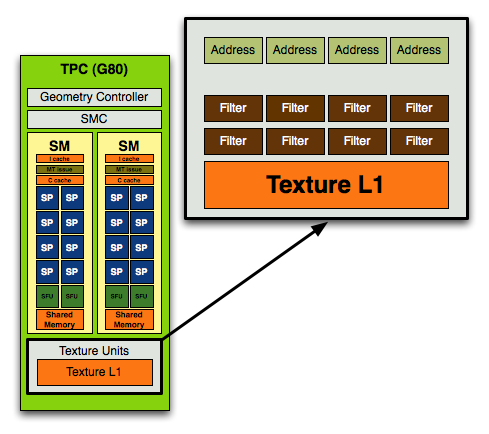
In each block you had 4 texture address units and 8 texture filtering units.
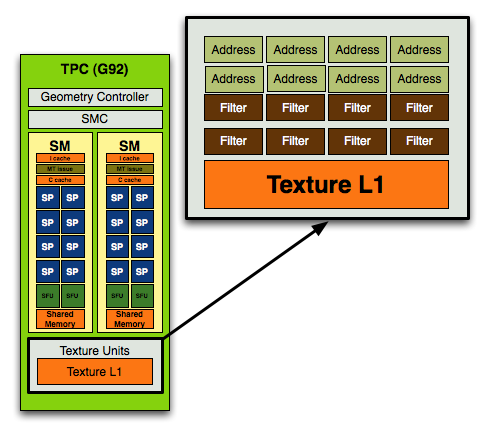
With the move to G92, used in the GeForce 8800 GT, 8800 GTS 512 and 9800 GTX, NVIDIA doubled the number of texture address units and achieved a 1:1 ratio of address/filtering units:
With GT200 in the GeForce GTX 280/260, NVIDIA kept the address-to-filtering ratio at 1:1 but increased the ratio of SPs to texture processors:
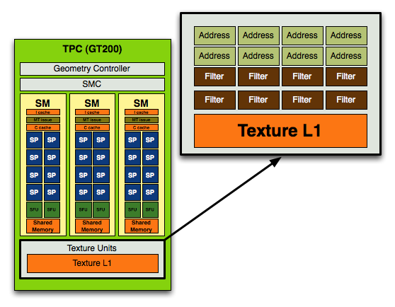
In the previous designs you'd have 8 address and 8 filtering units per TPC (or 16 streaming processors), in the GT200 you have the same 8 address and 8 filtering units but for a larger TPC with 24 SPs.
Here's how the specs stand up across the generations:
| NVIDIA Architecture Comparison | G80 | G92 | GT200 |
| Streaming Processors per TPC | 16 | 16 | 24 |
| Texture Address Units per TPC | 4 | 8 | 8 |
| Texture Filtering Units per TPC | 8 | 8 | 8 |
| Total SPs | 128 | 128 | 240 |
| Total Texture Address Units | 32 | 64 | 80 |
| Total Texture Filtering Units | 64 | 64 | 80 |
For a 87.5% increase in compute, there's a mere 25% increase in texture processing power. This ratio echoes what NVIDIA has been preaching for years: that games are running more complex shaders and are not as bound by texture processing as they were in years prior. If this wasn't true then we'd see a closer to 25% increase in performance of GT200 over G80 at the same clock rather than something much greater.
It also means that GT200's performance advantage over G80 or G92 based architectures (e.g. GeForce 9800 GTX) will be determined much by how computationally bound the games we're testing are.
The ratio of increase compute/texture power in the GT200 has been evident in NVIDIA architectures for years now, dating back to the ill-fated GeForce FX. NVIDIA sacrificed memory bandwidth on the GeForce FX, equipping it with a narrow 128-bit memory bus (compared to ATI's 256-bit interface on the Radeon 9700 Pro) and instead focused on building a much more powerful compute engine. Unfortunately, the bet was the wrong one to make at the time and the GeForce FX was hardly competitive (for more reasons than just a lack of memory bandwidth), but today we're dealing in a very different world. Complex shader programs run on each pixel on the screen and there's a definite need for more compute power in today's GPUs.
An Increase in Rasterization Throughput
In addition to the 25% increase in texture processing capabilities of the GT200, NVIDIA added two more ROP partitions to the GPU. While the GeForce 8800 GTX had six ROP partitions, each capable of outputting a maximum of 4 pixels per clock, the GT200 adds two more partitions.
With eight ROP partitions the GT200 can now output a maximum of 32 pixels per clock, up from 24 pixels per clock in the GeForce 8800 GTX and 9800 GTX.
The pixel blend rate on G80/G92 was half-speed, meaning that while you could output 24 pixels per clock, you could only blend 12 pixels per clock. Thanks to the 65nm shrink and redesign, GT200 can now output and blend pixels at full speed - that's 32 pixels per clock for each.
The end result is a non-linear performance improvement in everything from anti-aliasing and fire effects to shadows on GT200. It's an evolutionary change, but that really does sum up many of the enhancements of GT200 over G80/G92.


108 Comments
View All Comments
woofermazing - Tuesday, June 17, 2008 - link
Isn't the R700 high-end model going to have a direct link between the two cores. Could be a false rumor, but i would think that would solve a lot of problems with having two GPU's on a single board, since games would see it as 1 chip instead of a Crossfire/SLI setup. And besides, why the heck does it matter what the card looks like under the cooler. If it delivers better performance than Nvidia's offering without driver headaches, I don't think most gamers are going to care.VooDooAddict - Tuesday, June 17, 2008 - link
Why am I the only one happy about this product?Since the release of the 8800GTX top end single GPU performance has been a little stagnant... then came the refresh (8800GT/8800GTS-512) better prices came into effect.
Now we've got the new generation, and like in years prior, the new gen single GPU card has near performance of the previous gen in SLI. Price is also similar with when NVIDIA launched the first 8800GTX.
Sure, I wish they came in at a lower price point and at less power draw. (Same complaints that we had with the original 8800GTX). Lower power and lower price will come with a refresh.
Will I be getting one? ... nahh these cheap 9600GTs, overclocked 8800GT's and 8800GTSs will be the cards I recomend till i see the refresh. But I'm still happy there's progress.
I'm hoping the refresh hits around the same time as Intel's updated quad core.
DerekWilson - Tuesday, June 17, 2008 - link
i think its neat and has very interesting technology under the hood.but i'm not gonna spend that much money for something that doesn't deliver enough value (or even performance) compared to other solutions that are available. you pretty much reflect my own sentiment there: it's another step forward but not one that you're gonna buy.
i think people "don't like it" because of that though. it just isn't worth it right now and that's certainly valid.
greenx - Tuesday, June 17, 2008 - link
There are two ways I can look at this article.1)First an foremost at the heart of a real gamer ticks the need for good story lines fed by characters you will never forget, held by a gameplay you will fall in love with and finally covered by graphics that will transport you to another world (kinda like when I first played FF VII on my PC).
Within the context of the world we live in today I wonder what is really going through the minds of these people selling $600+ video cards. Kinda like those $10 000+ PCs. Madness. Sure they have their market up there but I shudder to think of how much money has been poured into appeasing a select few. Furthermore for what reason? Glory? I don't know but seeing as how the average gamer is what has made the PC/Gaming scene what it is, where does a $600+ video card fit into the grand scheme of things?
2) The possibilities that these new cards open up certainly seem exciting. The comparison with intel has been justified, but considering the other alternatives out there are much further ahead in development, who is going to bypass intel/amd/etc for a GPU technology based supercomputer?
DerekWilson - Tuesday, June 17, 2008 - link
two address point 2):developers will bypass Intel, AMD, SUN, whoever owns Cray these days, and all other HPC developers when a technology comes along that can speed up their applications by two orders of magnitude immediately on hardware that costs thousands (and in large cases millions) less to build, run and develop for.
evolucion8 - Tuesday, June 17, 2008 - link
LOL that was quite funny but incorrect as well, there's more than 4 Billion of people in China, in the future probably nVidia will launch a 4 Billion Transistors GPU hehe. It will require a Nuclear Reactor to turn it on, a and two of them to play games :D7Enigma - Wednesday, June 18, 2008 - link
4 Billion? Did you just make that out of thin air. Latest tabs show approximately 1.4 billion (give or take a couple hundred million). The world population is only estimated at 6.6 billion, so unless 60% of the people in the world are living in China, you're clueless.http://geography.about.com/od/populationgeography/...">http://geography.about.com/od/populationgeography/...
Bahadir - Tuesday, June 17, 2008 - link
Firstly I must say I enjoyed reading the whole article written by Anand Lal Shimpi & Derek Wilson. However, what does not make sense to me is the fact that "At most, 105 NVIDIA GT200 die can be produced on a single 300mm 65nm wafer from TSMC", but by looking at the wafer, only 95 full dies can be seen. Is this the wrong die?Also, it is not fair to compare the die of the Penryn against the GTX 280die because Penryn's die was made in 45nm process and GTX280 was made in 65nm die. Maybe it would be fair to compare it with the Conroe (65nm) die. But well done folks for putting an excellent article together!
Anand Lal Shimpi - Tuesday, June 17, 2008 - link
Thanks for your kind words btw :) Both of us really appreciate it - same to everyone else in this thread, thanks for making a ridiculously long couple of weeks (and a VERY long night) worth it :)-A
Anand Lal Shimpi - Tuesday, June 17, 2008 - link
You're right, there's actually a maximum of 94 usable die per wafer :)Take care,
Anand