NVIDIA's 1.4 Billion Transistor GPU: GT200 Arrives as the GeForce GTX 280 & 260
by Anand Lal Shimpi & Derek Wilson on June 16, 2008 9:00 AM EST- Posted in
- GPUs
Building NVIDIA's GT200
Here's a Streaming Processor, NVIDIA calls it an SP:
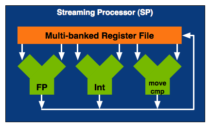
NVIDIA calls an individual SP a single processing core, which is actually true. It is a fully pipelined, single-issue, in-order microprocessor complete with two ALUs and a FPU. An SP doesn't have any cache, so it's not particularly great at anything other than cranking through tons of mathematical operations. Since an SP spends most of its time working on pixel or vertex data, the fact that it doesn't have a cache doesn't really matter. Aside from name similarities, one NVIDIA SP is a lot like a very simplified version of a SPE in the Cell microprocessor (or maybe the SPE is like a really simple version of one of NVIDIA's SMs, which we'll get to in a minute). While a single SPE in Cell has seven execution units, a single NVIDIA SP only has three.
By itself a SP is fairly useless, but NVIDIA builds GPUs and if you add up enough of these little monsters you can start to get something productive given that graphics rendering is a highly parallelizable task.
Here's a Streaming Multiprocessor, which NVIDIA abbreviates as SM:

A SM is an array of SPs, eight to be specific, along with two more processors called Special Function Units (SFUs). Each SFU has four FP multiply units which are used for transcendental operations (e.g. sin, cosin) and interpolation, the latter being used in some of the calculations for things like anisotropic texture filtering. Although NVIDIA isn't specific in saying so, we assume that each SFU is also a fully pipelined, single-issue, in-order microprocessor. There's a MT issue unit that dispatches instructions to all of the SPs and SFUs in the group.
In addition to the processor cores in a SM, there's a very small instruction cache, a read only data cache and a 16KB read/write shared memory. These cache sizes are kept purposefully small because unlike a conventional desktop microprocessor, the datasets we're trying to cache here are small. Each SP ends up working on an individual pixel and despite the move to 32-bit floating point values, there's only so much data associated with a single pixel. The 16KB memory is akin to Cell's local stores in that it's not a cache, but a software-managed data store so that latency is always predictable. With this many cores in a single SM, control and predictability and very important to making the whole thing work efficiently.
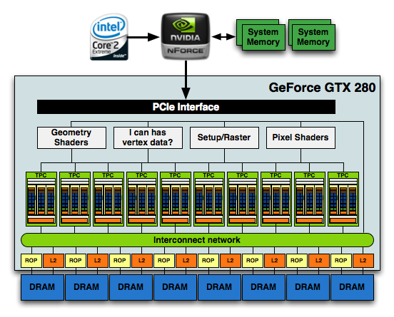
Take one more step back and you've got a Texture/Processor Cluster (TPC):
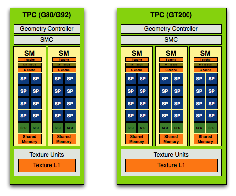
The G80/G92 TPC (left) vs. the GT200 TPC (right)
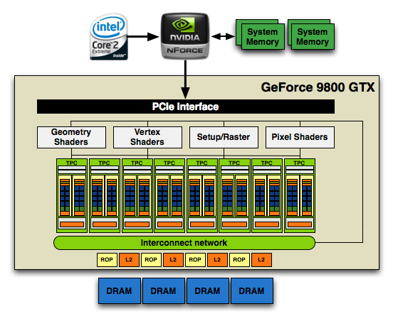
NVIDIA purposefully designed its GPU architecture to be modular, so a single TPC can be made up of any number of SMs. In the G80 architecture it was made up of two SMs but with the GT200 architecture it now has three SMs.
The components of the TPC however haven't changed; a TPC is made up of SMs, some control logic and a texture block. Remember that a SM is a total of 8 SPs and 2 SFUs, so that brings the total up to 24 SPs and 6 SFUs (must...not...type...STFU) per cluster in GT200 (up from 16 SPs and 4 SFUs in G80). The texture block includes texture addressing and filtering logic as well as a L1 texture cache.
The modular theme continues with the Streaming Processor Array (SPA) that is composed of a number of TPCs:
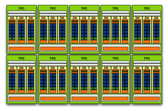
The GT200 SPA, that's 240 SPs in there if you want to count them
In G80 the SPA was made up of 8 TPCs, but with GT200 we've moved up to 10. Note that each TPC now has 3 SMs vs. 2, so the overall processing power of GT200 has increased by 87.5% over G80.
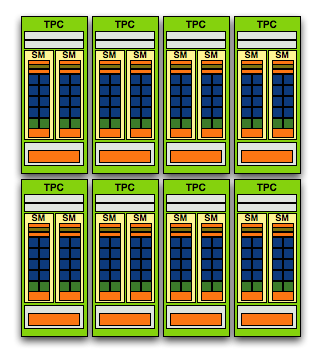
And here's G80/G92, only 128 SPs thanks to two SMs per TPC and 8 TPCs
At the front end of the GPU we've got schedulers and control logic to distribute workloads to the entire array of processing cores. At the other end we've got L2 texture caches and rasterization processors that handle final filtering and output of data to the frame buffer.
The culmination of all of this is that the new GT200 GPU, the heart of the GeForce GTX 280 and 260, features 240 SPs, 160KB of local memory, an even smaller amount of cache and is built on TSMC's 65nm process using 1.4 billion transistors.
1.4 Billion Transistors. It wants vertex data. Really bad.
754 Million Transistors
There are more transistors in this chip than there are people in China, and it's the largest, most compute-dense chip we've ever reviewed.


108 Comments
View All Comments
woofermazing - Tuesday, June 17, 2008 - link
Isn't the R700 high-end model going to have a direct link between the two cores. Could be a false rumor, but i would think that would solve a lot of problems with having two GPU's on a single board, since games would see it as 1 chip instead of a Crossfire/SLI setup. And besides, why the heck does it matter what the card looks like under the cooler. If it delivers better performance than Nvidia's offering without driver headaches, I don't think most gamers are going to care.VooDooAddict - Tuesday, June 17, 2008 - link
Why am I the only one happy about this product?Since the release of the 8800GTX top end single GPU performance has been a little stagnant... then came the refresh (8800GT/8800GTS-512) better prices came into effect.
Now we've got the new generation, and like in years prior, the new gen single GPU card has near performance of the previous gen in SLI. Price is also similar with when NVIDIA launched the first 8800GTX.
Sure, I wish they came in at a lower price point and at less power draw. (Same complaints that we had with the original 8800GTX). Lower power and lower price will come with a refresh.
Will I be getting one? ... nahh these cheap 9600GTs, overclocked 8800GT's and 8800GTSs will be the cards I recomend till i see the refresh. But I'm still happy there's progress.
I'm hoping the refresh hits around the same time as Intel's updated quad core.
DerekWilson - Tuesday, June 17, 2008 - link
i think its neat and has very interesting technology under the hood.but i'm not gonna spend that much money for something that doesn't deliver enough value (or even performance) compared to other solutions that are available. you pretty much reflect my own sentiment there: it's another step forward but not one that you're gonna buy.
i think people "don't like it" because of that though. it just isn't worth it right now and that's certainly valid.
greenx - Tuesday, June 17, 2008 - link
There are two ways I can look at this article.1)First an foremost at the heart of a real gamer ticks the need for good story lines fed by characters you will never forget, held by a gameplay you will fall in love with and finally covered by graphics that will transport you to another world (kinda like when I first played FF VII on my PC).
Within the context of the world we live in today I wonder what is really going through the minds of these people selling $600+ video cards. Kinda like those $10 000+ PCs. Madness. Sure they have their market up there but I shudder to think of how much money has been poured into appeasing a select few. Furthermore for what reason? Glory? I don't know but seeing as how the average gamer is what has made the PC/Gaming scene what it is, where does a $600+ video card fit into the grand scheme of things?
2) The possibilities that these new cards open up certainly seem exciting. The comparison with intel has been justified, but considering the other alternatives out there are much further ahead in development, who is going to bypass intel/amd/etc for a GPU technology based supercomputer?
DerekWilson - Tuesday, June 17, 2008 - link
two address point 2):developers will bypass Intel, AMD, SUN, whoever owns Cray these days, and all other HPC developers when a technology comes along that can speed up their applications by two orders of magnitude immediately on hardware that costs thousands (and in large cases millions) less to build, run and develop for.
evolucion8 - Tuesday, June 17, 2008 - link
LOL that was quite funny but incorrect as well, there's more than 4 Billion of people in China, in the future probably nVidia will launch a 4 Billion Transistors GPU hehe. It will require a Nuclear Reactor to turn it on, a and two of them to play games :D7Enigma - Wednesday, June 18, 2008 - link
4 Billion? Did you just make that out of thin air. Latest tabs show approximately 1.4 billion (give or take a couple hundred million). The world population is only estimated at 6.6 billion, so unless 60% of the people in the world are living in China, you're clueless.http://geography.about.com/od/populationgeography/...">http://geography.about.com/od/populationgeography/...
Bahadir - Tuesday, June 17, 2008 - link
Firstly I must say I enjoyed reading the whole article written by Anand Lal Shimpi & Derek Wilson. However, what does not make sense to me is the fact that "At most, 105 NVIDIA GT200 die can be produced on a single 300mm 65nm wafer from TSMC", but by looking at the wafer, only 95 full dies can be seen. Is this the wrong die?Also, it is not fair to compare the die of the Penryn against the GTX 280die because Penryn's die was made in 45nm process and GTX280 was made in 65nm die. Maybe it would be fair to compare it with the Conroe (65nm) die. But well done folks for putting an excellent article together!
Anand Lal Shimpi - Tuesday, June 17, 2008 - link
Thanks for your kind words btw :) Both of us really appreciate it - same to everyone else in this thread, thanks for making a ridiculously long couple of weeks (and a VERY long night) worth it :)-A
Anand Lal Shimpi - Tuesday, June 17, 2008 - link
You're right, there's actually a maximum of 94 usable die per wafer :)Take care,
Anand