NVIDIA's 1.4 Billion Transistor GPU: GT200 Arrives as the GeForce GTX 280 & 260
by Anand Lal Shimpi & Derek Wilson on June 16, 2008 9:00 AM EST- Posted in
- GPUs
One-Point-Four-Billion. That's transistors folks.
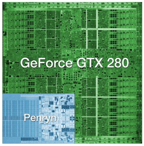
The chip is codenamed GT200 and it's the successor to NVIDIA's G80 and G92 families. Why the change in naming? The GT stands for "Graphics Tesla" and this is the second generation Graphics Tesla architecture, the first being the G80. The GT200 is launching today in two flavors, the die of the larger one is pictured below:
Um...yeah...we're reviewing that today
(this die comparison is to scale and that's a dual-core Penryn)
Let's put aside all the important considerations for a moment and bask in the glow of sheer geekdom. Intel's Montecito processor (their dual core Itanium 2) weighs in at over 1.7 billion transistors, but the vast majority of this is L3 cache (over 1.5 billion transistors for 24MB of on die memory). In contrast, the vast majority of the transistors on NVIDIA's GT200 chip are used for compute power. Whether or not NVIDIA has used these transistors well is certainly the most important consideration for consumers, but there's no reason we can't take a second to be in awe of the sheer magnitude of the hardware. This chip is packed full of logic and it is huge.
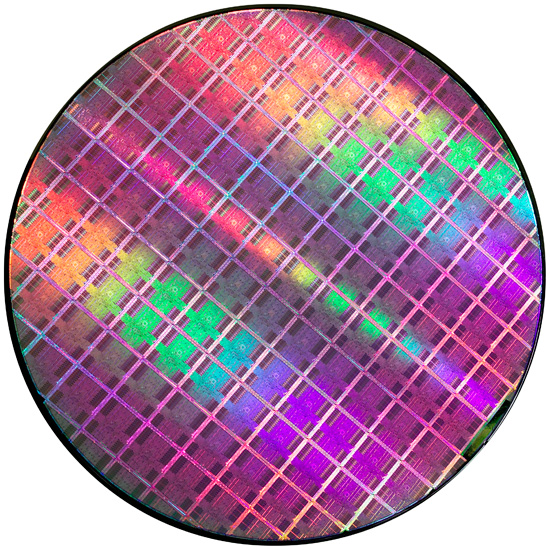
At most, 94 NVIDIA GT200 die can be produced on a single 300mm 65nm wafer from TSMC. On the other end of the spectrum, Intel can fit around 2500 45nm Atom processors on a 300mm wafer.
If the number of transistors wasn't enough to turn this thing into a dinner plate sized bit of hardware, the fact that it's fabbed on a 65nm process definitely puts it over the top. Current CPUs are at 45nm and NVIDIA's major competitor in the GPU market, AMD, has been building 55nm graphics chips for over 7 months now. With so many transistors, choosing not to shrink their manufacturing process doesn't seem to make much sense to us. Smaller fab processes offer not only the potential for faster, cooler chips, but also significantly reduce the cost of the GPU itself. Because manufacturing costs are (after ramping production) on a per wafer basis, the more dies that can be packed onto a single waffer, the less each die costs. It is likely that NVIDIA didn't want to risk any possible delays arising from manufacturing process changes on this cycle, but that seems like a risk that would have been worth taking in this case.
Instead, GT200 is the largest die TSMC has ever fabbed for production. Quite a dubious honor, and I wouldn't expect NVIDIA to really see this as something of which to be proud. Of course, that doesn't mean we can't be impressed with the sheer massiveness of the beast.
And what do we get from all these transistors? Moving up from 690M transistors of the original G80 and 754M transistors in G92 to the 1.4B transistors of GT200 is not a small tweak. One of the major new features is the ability to processes double precision floating point data in hardware (there are 30 64-bit FP units in GT200). The size of the register file for each SP array has been doubled. The promised ability of an SP to process a MAD and a MUL at the same time has been enhanced to work in more cases (G80 was supposedly able to do this, but the number of cases where it worked as advertised were extremely limited). And the number of SPs has increased from 128 on G80 to 240 with GT200. To better understand what all this means, we'll take a closer look at the differences between G80 and GT200, but first, the cards.
Clock Speeds, Pricing and HDMI Information
NVIDIA is introducing two GT200 parts today along with slightly tweaked branding. The new brand is called the GeForce GTX, and the first two cards are the GTX 280 and GTX 260.


Here's the card, say hello:
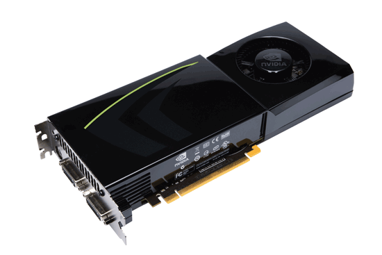
The GeForce GTX 280
It's got a little sibling too:

The GeForce GTX 260
The GeForce GTX 280 features 240 streaming processors running at 1.3GHz. It's got a 512-bit memory interface to 1GB of GDDR3 running at 2.2GHz (1107MHz core clock). The rest of the GPU runs at 602MHz.
| |
GTX 280 | GTX 260 | 9800 GX2 | 9800 GTX | 8800 GTS 512 | 8800 GT |
| Stream Processors | 240 | 192 | 256 | 128 | 128 | 112 |
| Texture Address / Filtering | 80 / 80 | 64 / 64 | 128 / 128 | 64 / 64 | 56 / 56 | 56 / 56 |
| ROPs | 32 | 28 | 32 | 16 | 16 | 16 |
| Core Clock | 602MHz | 576MHz | 600MHz | 675MHz | 650MHz | 600MHz |
| Shader Clock | 1296MHz | 1242MHz | 1500MHz | 1690MHz | 1625MHz | 1500MHz |
| Memory Clock | 1107MHz | 999MHz | 1000MHz | 1100MHz | 970MHz | 900MHz |
| Memory Bus Width | 512-bit | 448-bit | 256-bit x 2 | 256-bit | 256-bit | 256-bit |
| Frame Buffer | 1GB | 896MB | 1GB | 512MB | 512MB | 512MB |
| Transistor Count | 1.4B | 1.4B | 1.5B | 754M | 754M | 754M |
| Manufacturing Process | TSMC 65nm | TSMC 65nm | TSMC 65nm | TSMC 65nm | TSMC 65nm | TSMC 65nm |
| Price Point | $650 | $400 | $500 | $300 | $280 | $170-$230 |
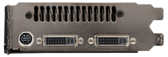
You'll need a power supply that can deliver up to 236W for the card itself and you'll need both a 6-pin and an 8-pin PCIe power connector (the board won't work with two 6-pin connectors).
The GeForce GTX 280 will retail for $650 with availability planned for June 17th.
The GTX 260 brings the total core count down to 192 by disabling two Texture/Processing Clusters on the GPU (but still maintaining more cores than any single-GPU G80/G92 based card). The SPs run slightly slower on the GTX 260 (1242MHz vs. 1296MHz, NVIDIA uses a 27MHz crystal so that's why we get these funny clock frequencies), while the memory runs at approximately 2GHz (999MHz memory clock, 1998MHz data rate). The GTX 260 also loses one of the 8 64-bit memory controllers, bringing the total memory bus down to 448-bits and total memory size down to 896MB.
The GTX 260 consumes a maximum of 183W and only needs two 6-pin power connectors. The GeForce GTX 260 will set you back $400 and should be available on June 26th.
The GTX 280's shroud, though it takes some cues from the 9800 GX2, is better engineered to allow for heat expulsion through a larger vent next to the IO ports. The 9800 GX2 didn't have a very wide opening to the outside world from which to remove heat. This resulted in the 9800 GX2 disproportionately increasing the heat of the system. Since we run our systems without cases we don't see problems like this as soon as our readers do, and we would like to thank you for pointing this out to us.
Both the GTX 260 and 280 have two dual-link DVI outputs, which can be converted to HDMI using an adapter if you'd like. You can pass SPDIF using a connector at the top of the card, which will then be passed to the HDMI output when using the DVI-HDMI adapter. For the HTPC enthusiasts out there, the GTX 280 and 260 can output the following audio formats over HDMI:
2-channel LPCM
6-channel DD bitstream
6-channel DTS bitstream
Unfortunately there's no support for 8-channel LPCM or bitstreaming of Dolby TrueHD or DTS HD-MA.


108 Comments
View All Comments
woofermazing - Tuesday, June 17, 2008 - link
Isn't the R700 high-end model going to have a direct link between the two cores. Could be a false rumor, but i would think that would solve a lot of problems with having two GPU's on a single board, since games would see it as 1 chip instead of a Crossfire/SLI setup. And besides, why the heck does it matter what the card looks like under the cooler. If it delivers better performance than Nvidia's offering without driver headaches, I don't think most gamers are going to care.VooDooAddict - Tuesday, June 17, 2008 - link
Why am I the only one happy about this product?Since the release of the 8800GTX top end single GPU performance has been a little stagnant... then came the refresh (8800GT/8800GTS-512) better prices came into effect.
Now we've got the new generation, and like in years prior, the new gen single GPU card has near performance of the previous gen in SLI. Price is also similar with when NVIDIA launched the first 8800GTX.
Sure, I wish they came in at a lower price point and at less power draw. (Same complaints that we had with the original 8800GTX). Lower power and lower price will come with a refresh.
Will I be getting one? ... nahh these cheap 9600GTs, overclocked 8800GT's and 8800GTSs will be the cards I recomend till i see the refresh. But I'm still happy there's progress.
I'm hoping the refresh hits around the same time as Intel's updated quad core.
DerekWilson - Tuesday, June 17, 2008 - link
i think its neat and has very interesting technology under the hood.but i'm not gonna spend that much money for something that doesn't deliver enough value (or even performance) compared to other solutions that are available. you pretty much reflect my own sentiment there: it's another step forward but not one that you're gonna buy.
i think people "don't like it" because of that though. it just isn't worth it right now and that's certainly valid.
greenx - Tuesday, June 17, 2008 - link
There are two ways I can look at this article.1)First an foremost at the heart of a real gamer ticks the need for good story lines fed by characters you will never forget, held by a gameplay you will fall in love with and finally covered by graphics that will transport you to another world (kinda like when I first played FF VII on my PC).
Within the context of the world we live in today I wonder what is really going through the minds of these people selling $600+ video cards. Kinda like those $10 000+ PCs. Madness. Sure they have their market up there but I shudder to think of how much money has been poured into appeasing a select few. Furthermore for what reason? Glory? I don't know but seeing as how the average gamer is what has made the PC/Gaming scene what it is, where does a $600+ video card fit into the grand scheme of things?
2) The possibilities that these new cards open up certainly seem exciting. The comparison with intel has been justified, but considering the other alternatives out there are much further ahead in development, who is going to bypass intel/amd/etc for a GPU technology based supercomputer?
DerekWilson - Tuesday, June 17, 2008 - link
two address point 2):developers will bypass Intel, AMD, SUN, whoever owns Cray these days, and all other HPC developers when a technology comes along that can speed up their applications by two orders of magnitude immediately on hardware that costs thousands (and in large cases millions) less to build, run and develop for.
evolucion8 - Tuesday, June 17, 2008 - link
LOL that was quite funny but incorrect as well, there's more than 4 Billion of people in China, in the future probably nVidia will launch a 4 Billion Transistors GPU hehe. It will require a Nuclear Reactor to turn it on, a and two of them to play games :D7Enigma - Wednesday, June 18, 2008 - link
4 Billion? Did you just make that out of thin air. Latest tabs show approximately 1.4 billion (give or take a couple hundred million). The world population is only estimated at 6.6 billion, so unless 60% of the people in the world are living in China, you're clueless.http://geography.about.com/od/populationgeography/...">http://geography.about.com/od/populationgeography/...
Bahadir - Tuesday, June 17, 2008 - link
Firstly I must say I enjoyed reading the whole article written by Anand Lal Shimpi & Derek Wilson. However, what does not make sense to me is the fact that "At most, 105 NVIDIA GT200 die can be produced on a single 300mm 65nm wafer from TSMC", but by looking at the wafer, only 95 full dies can be seen. Is this the wrong die?Also, it is not fair to compare the die of the Penryn against the GTX 280die because Penryn's die was made in 45nm process and GTX280 was made in 65nm die. Maybe it would be fair to compare it with the Conroe (65nm) die. But well done folks for putting an excellent article together!
Anand Lal Shimpi - Tuesday, June 17, 2008 - link
Thanks for your kind words btw :) Both of us really appreciate it - same to everyone else in this thread, thanks for making a ridiculously long couple of weeks (and a VERY long night) worth it :)-A
Anand Lal Shimpi - Tuesday, June 17, 2008 - link
You're right, there's actually a maximum of 94 usable die per wafer :)Take care,
Anand