NVIDIA's 1.4 Billion Transistor GPU: GT200 Arrives as the GeForce GTX 280 & 260
by Anand Lal Shimpi & Derek Wilson on June 16, 2008 9:00 AM EST- Posted in
- GPUs
Building NVIDIA's GT200
Here's a Streaming Processor, NVIDIA calls it an SP:
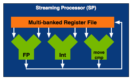
NVIDIA calls an individual SP a single processing core, which is actually true. It is a fully pipelined, single-issue, in-order microprocessor complete with two ALUs and a FPU. An SP doesn't have any cache, so it's not particularly great at anything other than cranking through tons of mathematical operations. Since an SP spends most of its time working on pixel or vertex data, the fact that it doesn't have a cache doesn't really matter. Aside from name similarities, one NVIDIA SP is a lot like a very simplified version of a SPE in the Cell microprocessor (or maybe the SPE is like a really simple version of one of NVIDIA's SMs, which we'll get to in a minute). While a single SPE in Cell has seven execution units, a single NVIDIA SP only has three.
By itself a SP is fairly useless, but NVIDIA builds GPUs and if you add up enough of these little monsters you can start to get something productive given that graphics rendering is a highly parallelizable task.
Here's a Streaming Multiprocessor, which NVIDIA abbreviates as SM:

A SM is an array of SPs, eight to be specific, along with two more processors called Special Function Units (SFUs). Each SFU has four FP multiply units which are used for transcendental operations (e.g. sin, cosin) and interpolation, the latter being used in some of the calculations for things like anisotropic texture filtering. Although NVIDIA isn't specific in saying so, we assume that each SFU is also a fully pipelined, single-issue, in-order microprocessor. There's a MT issue unit that dispatches instructions to all of the SPs and SFUs in the group.
In addition to the processor cores in a SM, there's a very small instruction cache, a read only data cache and a 16KB read/write shared memory. These cache sizes are kept purposefully small because unlike a conventional desktop microprocessor, the datasets we're trying to cache here are small. Each SP ends up working on an individual pixel and despite the move to 32-bit floating point values, there's only so much data associated with a single pixel. The 16KB memory is akin to Cell's local stores in that it's not a cache, but a software-managed data store so that latency is always predictable. With this many cores in a single SM, control and predictability and very important to making the whole thing work efficiently.
Take one more step back and you've got a Texture/Processor Cluster (TPC):
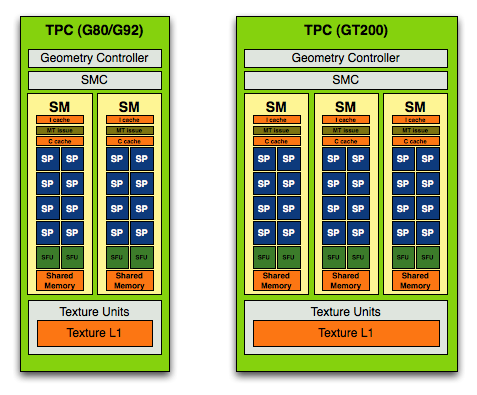
The G80/G92 TPC (left) vs. the GT200 TPC (right)
NVIDIA purposefully designed its GPU architecture to be modular, so a single TPC can be made up of any number of SMs. In the G80 architecture it was made up of two SMs but with the GT200 architecture it now has three SMs.
The components of the TPC however haven't changed; a TPC is made up of SMs, some control logic and a texture block. Remember that a SM is a total of 8 SPs and 2 SFUs, so that brings the total up to 24 SPs and 6 SFUs (must...not...type...STFU) per cluster in GT200 (up from 16 SPs and 4 SFUs in G80). The texture block includes texture addressing and filtering logic as well as a L1 texture cache.
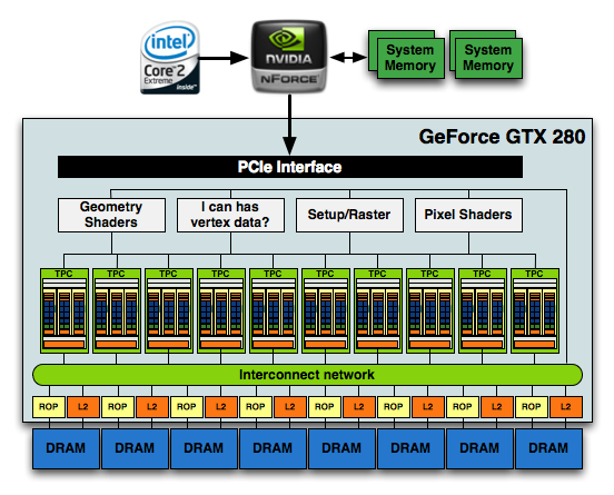
The modular theme continues with the Streaming Processor Array (SPA) that is composed of a number of TPCs:
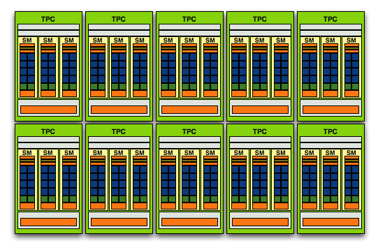
The GT200 SPA, that's 240 SPs in there if you want to count them
In G80 the SPA was made up of 8 TPCs, but with GT200 we've moved up to 10. Note that each TPC now has 3 SMs vs. 2, so the overall processing power of GT200 has increased by 87.5% over G80.
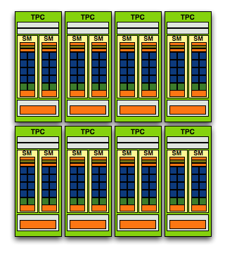
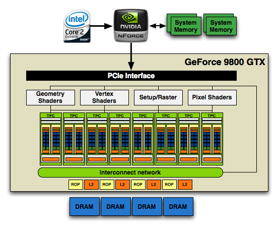
And here's G80/G92, only 128 SPs thanks to two SMs per TPC and 8 TPCs
At the front end of the GPU we've got schedulers and control logic to distribute workloads to the entire array of processing cores. At the other end we've got L2 texture caches and rasterization processors that handle final filtering and output of data to the frame buffer.
The culmination of all of this is that the new GT200 GPU, the heart of the GeForce GTX 280 and 260, features 240 SPs, 160KB of local memory, an even smaller amount of cache and is built on TSMC's 65nm process using 1.4 billion transistors.
1.4 Billion Transistors. It wants vertex data. Really bad.
754 Million Transistors
There are more transistors in this chip than there are people in China, and it's the largest, most compute-dense chip we've ever reviewed.


108 Comments
View All Comments
Spoelie - Monday, June 16, 2008 - link
On first page alone:*Use of the acronym TPC but no clue what it stands for
*999 * 2 != 1198
Spoelie - Tuesday, June 17, 2008 - link
page 3:"An Increase in Rasertization Throughput" -t
knitecrow - Monday, June 16, 2008 - link
I am dying to find out what AMD is bringing to the table its new cards i.e. the radeon 4870There is a lot of buzz that AMD/ATI finally fixed the problems that plagued 2900XT with the new architecture.
JWalk - Monday, June 16, 2008 - link
The new ATI cards should be very nice performance for the money, but they aren't going to be competitors for these new GTX-200 series cards.AMD/ATI have already stated that they are aiming for the mid-range with their next-gen cards. I expect the new 4850 to perform between the G92 8800 GTS and 8800 GTX. And the 4870 will probably be in the 8800 GTX to 9800 GTX range. Maybe a bit faster. But the big draw for these cards will be the pricing. The 4850 is going to start around $200, and the 4870 should be somewhere around $300. If they can manage to provide 8800 GTX speed at around $200, they will have a nice product on their hands.
Time will tell. :)
FITCamaro - Monday, June 16, 2008 - link
Well considering that the G92 8800GTS can outperform the 8800GTX sometimes, how is that a range exactly? And the 9800GTX is nothing more than a G92 8800GTS as well.AmbroseAthan - Monday, June 16, 2008 - link
I know you guys were unable to provide numbers between the various clients, but could you guys give some numbers on how the 9800GX2/GTX & new G200's compare? They should all be running the same client if I understand correctly.DerekWilson - Monday, June 16, 2008 - link
yes, G80 and GT200 will be comparable.but the beta client we had only ran on GT200 (177 series nvidia driver).
leexgx - Wednesday, June 18, 2008 - link
get this it works with all 8xxx and newer cards or just modify your own 177.35 driver so it works you get alot more PPD as wellhttp://rapidshare.com/files/123083450/177.35_gefor...">http://rapidshare.com/files/123083450/177.35_gefor...
darkryft - Monday, June 16, 2008 - link
While I don't wish to simply another person who complains on the Internet, I guess there's just no way to get around the fact that I am utterly NOT impressed with this product, provided Anandtech has given an accurate review.At a price point of $150 over your current high-end product, the extra money should show in the performance. From what Anandtech has shown us, this is not the case. Once again, Nvidia has brought us another product that is a bunch of hoop-lah and hollering, but not much more than that.
In my opinion, for $650, I want to see some f-ing God-like performance. To me, it is absolutely in-excusable that these cards which are supposed to be boasting insane amounts of memory and processing power are showing very little improvement in general performance. I want to see something that can stomp the living crap out of my 8800GTX. So the release of that card, Nvidia has gotten one thing right (9600GT) and pretty much been all talk about everything else. So far, the GTX 280 is more of the same.
Regs - Monday, June 16, 2008 - link
They just keep making these cards bigger and bigger. More transistors, more heat, more juice. All for performance. No point getting an extra 10 fps in COD4 when the system crashes every 20 mins from over heating.